Thursday, April 22nd, 2010
HP Labs in Palo Alto has been leading the development of the “memristor,” and researchers there have finally discovered the underlying mechanism for the formation of devices that can function as memory cells, logic circuits, and potentially even real artificial intelligence (AI)! Disclosing these results in his plenary speech to the attendees at the Nanocontacts and Nanointerconnects Workshop at the Spring 2010 Materials Research Society meeting on April 5th in San Francisco, HP Labs group leader Stan Williams (figure) explained how to make memristors without use of the hitherto-uncontrollable “electroforming” step.
At the risk of oversimplifying, a memristor can be thought of as a complex oxide sandwiched between two metal contacts, where the electrical resistance of the oxide changes due to current-flux induced ion drift that forms conductive filaments. Memristors were famously predicted in theory in 1971 by Leon Chua of U.C. Berkeley (Ref: IEEE Trans Circuit Theory 18, 507-519; 1971), yet theory provided no clues for practice, and it was only in 2008 that the Williams Group proved the function in oxides of titanium. “Leon Chua is the Albert Einstein of circuit theory,” declared Williams.
One of the biggest problems with HVM of memristor circuits had been that PVD of pure “rutile” (TiO2) titania results in simple resistors. Before these simple static resistors can become dynamic memristors, they have to be “electroformed” using a strong voltage-current applied for a minimum time. Electroforming was known to induce movements of ions and defects in the oxide, but we did not really know what final structure was created, and so could not begin to control the process so as to be able to integrate it into a complete device HVM flow.
“We spent ten years messing around making all the wrong measurements and coming to all the wrong conclusions before we discovered that these things are memristors, and we had to do time-dependent measurements,” explained Williams.
Williams’ Group at HP finally went through great expense and effort, networking with U.S. government labs for access to nanoscale materials characterization tools, to dissect memristors pre- and post-electroforming to determine what was happening at the atomic level. They found that electroforming was reducing the rutile TiO2 to a single-crystal of “magneli phase” Ti4O7 under each contact. For large area contacts, the Ti4O7 always appeared like a ~100nm diameter nanoscale plug relatively independent of the contact area, since essentially all the current flowed through this one plug during electroforming.
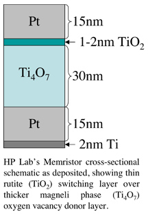
At geometries near optimal for memristor function, a 1-2nm thin TiO2 layer remained as a tunnel barrier. The width of the tunnel barrier then changed by ~0.5nm by the movement of ions within the oxide during memristor function. The switching mechanism for the memristor is thus field-induced drift of positively charged O+ vacancies in TiO2 that controls the resistance of the film. The Ti4O7 functions as a source/sink of O+ vacancies to diffuse into and out of the TiO2. “This can be thought of as a condensed phase of vacancies in TiO2,” according to Williams.
With this new understanding, Williams’ Group was able to conceive of forming the final device structure without having to electroform. Sourcing a new Ti4O7 PVD target, they now sputter 25-30nm of Ti4O7 followed by 1-2nm of standard TiO2 between ~15nm thick Pt electrodes (figure). To avoid oxidation of the bottom Pt electrode, they discovered that a few nm of Ti deposited below the electrode provides sufficient Ti to diffuse through the Pt and pin any vacancies at the Pt/Ti4O7 interface.
Other oxides sandwiched between other metals can also become memristors. Tradeoffs in materials selection involve switching speeds, device lifetimes, and manufacturing costs. While HP has led the world in pursuing memristor technology using the Pt/TixOy/Pt stack, there has been a rush of global R&D in both academia and industry to explore other materials systems. Indeed, there were dozens of papers presented at the Spring MRS Meeting on devices based on ionic transport in oxides to controllably change the resistance, however all of the presentations seen by this editor included mention of electroforming as part of the manufacturing flow. While additional materials engineering is needed to create high-yielding memristor arrays in high-volume manufacturing (HVM), it looks like everyone now has to agree upon two facts:
• from a HVM perspective, non-electroforming is the only way to go, and
• from a design perspective, memristors are intrinsically dynamic devices.
Memristors for ReRAM
HP Labs has been working on the smallest possible memory elements using cross-bar architectures. At the types of fields you can put on a nanoscale device you have to be concerned with the potential for damage at contacts. Argonne National Lab is testing some of the HP Labs’ newest 20nm line/space crossbar structures, but it is not easy to push the limits of the nanoscale manufacturing. For example, impedance spectroscopy is not so useful, because in non-linear devices the whole concept of impedance is not even valid.
Despite the difficulty to dynamically measure memristors, now that they are not-so-difficult to make we can use static properties to make memory arrays. With the ability to switch the resistance quickly between relatively high and low static states, we can make random-access memory (RAM) cross-bar array circuits with densities that beat Flash for equal minimum critical dimension on chip.
The main limitation now holding fabs back from making high-yielding ReRAMs is probably the Pt electrodes. So far, noble metal contacts seem to be essential to prevent contact oxidation and parasitic resistances, and noble metal patterning generally requires “lift-off” integration which can be problematic in geometries smaller than several microns. Still, lift-off is easily controlled for larger geometries, and the use of sidewall spacers and sacrificial masking layers may allow for high-yielding extendibility to <20nm and smaller devices.
Memristors for logic
There is an ongoing need to be able to create ever faster devices that can “flop” as elements of logic circuits. As Ghavam Shahidi of IBM Research in Yorktown Heights, NY presented at the “Device Architecture: Ultimate Planar CMOS Limit and Sub-32nm Device Options” short course at IEDM 2009, the world now has the ability to create 12.64 TeraFLOP ICs, with ExaFLOP ICs imagined by the year 2020. Extrapolating today’s state-of-the-art planar CMOS IC parameters out to ExaFLOP requirements, the power consumption would be 100s of MW to a few GW (for reference, a nuclear reactor typically produces ~1GW). Massive memristor arrays could theoretically provide high-speed logic functions with dramatically reduced power consumption compared to CMOS.
Since the memristor is a dynamical device, it changes with time, and two equations are needed to describe the device. All measurements must be made explicitly over time; not on a curve tracer, but by creating a state and then watching how the state changes over time. For example, starting with a nominal 1ms electrical pulse, and then applying a smaller bias voltage.
With only one variable changing—the width of the tunnel gap from 1.2 to 1.8nm—HP’s researchers found that they can fit the barrier heights and all other parameters to classic I/V curves using the Simmons Equation. For the width of the tunnel barrier varying over this range, the potential needed to switch a memristor ON varied from -1.25 to –1.4V, and the potential needed to switch a memristor OFF varied from +3.0 to +5.5V.
HP Labs’ has already reported on relay logic (without gain), information-packet and redundant-wire concepts to allow for 100% information transfer through 90% functional connections, and configurable interconnect layers for ASIC/FPGA hybrid functionality. Adding all of these technologies together results in unprecedented capabilities to create new logic circuits with uniquely valuable capabilities.
Memristors for AI
Perhaps the most elusive value in logic ICs has been anything associated with artificial intelligence (AI). Despite decades of theory and grandstanding by proponents such as Marvin Minsky, AI in practice has seemingly failed to create even the simplest circuit that can learn. Perhaps binary logic is inherently inadequate for AI, but analog logic based on memristors could work. “Since our brains are made of memristors, the flood gate is now open for commercialization of computers that would compute like human brains, which is totally different from the von Neumann architecture underpinning all digital computers,” predicted Chua.
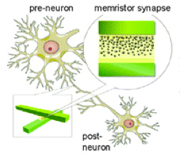
We now know that neuro-plasticity describes the ability of human neuronal networks to selectively form stronger or weaker connections as examples of adaptive learning. Neurons are triggered by ionic transport across the synaptic cleft—with nominal spacing <10nm (figure)—and since a neuron’s function varies with an “action potential” that creates non-linear dependencies, a memristor may be the closest solid-state electronic device we have found that mimics the function of a neuron.
Perhaps dense arrays of memristors could be somehow wired together to learn from inputs so as to create artificial intelligence (AI). Researchers in the Lu Group at the University of Michigan have already shown that, “a hybrid system composed of CMOS neurons and memristor synapses can support important synaptic functions such as spike timing dependent plasticity.” Maybe a massive memristor array will eventually be part of a system that will pass the Turing Test, and we’ll be one step closer to meeting Marvin the Paranoid Android. –E.K.
Tags: 16nm, 22nm, AI, logic, materials, memory, memristor, nano, R&D, ReRAM


