Wednesday, June 16th, 2010
While most of the IC manfacturing world has embraced the fabless/foundry split between design and manufacturing, Intel has remained staunchly vertically integrated and continues to reap the rewards. At the recent 2010 International Interconnect Technology Conference (IITC) in Burlingame, California, researchers from Intel confirmed that the design constraint of a fixed spacing between interconnect lines allows for the use of “air-gaps” in manufacturing to increase circuit speeds. While this approach has been considered for over 20 years, today no other company has all of it’s logic chip designs converted from anything-goes 2D to strict 1D layouts. Consequently, no other IC company can easily use this low-cost manufacturing trick today, even though EDA startup Tela Innovations has been selling gridded-design-rule (GDR) IP for a while now.

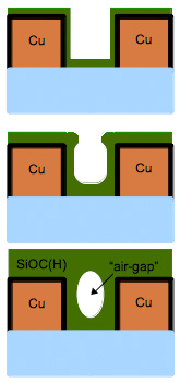
CVD can be easily tuned to initially coat sidewalls (top), then pinch-off (middle), and finally form a closed pore (bottom) during one step.
With shrinking IC sizes, the dielectric insulation between metal interconnects has become one of the major limits on increasing circuit speed, so the last 15 years has seen relentless pursuit of ever lower capacitance (“k” value) dielectric materials to replace SiO2 glass (k~4.0). Sadly, there are many devilish details of materials integration into nanometer-era ICs, and one by one the dozens of possible new low-k materials failed to meet specifications: too leaky, too soft, too unstable, and too expensive. The history of this debacle can be read in the wishful thinking specification for low-k dielectrics found in successive versions of the International Technology Roadmap for Semiconductors (ITRS) from 1998 to 2008. In 2010, with a few very limited exceptions, the only low-k dielectric used in commercial fabs is CVD SiOC(H) with k~3.0.
In fact, CVD SiOC(H) is such a good dielectric that nearly all attempts to reach k<2.5 now use this material as part of the final structure. Empirically, it has been found that nanometer-scale pores can be created in SiOC(H), and such porous low-k (PLK) films can get to ~10% porosity for a k~2.7 without too many problems. However, aiming for lower k-value generally results in connected pores that make soft and leaky and unstable films, and the work-arounds add expense and uncertainty. Still, as shown at IITC, most fabs are still pursuing work-arounds to strengthen, stabilize, and cap PLK films. In contast, Intel has chosen to add a single central pore to SiOC(H) so get to lower k (see figure).
To be clear, there is no “air” in what is not really a “gap” in an air-gap; it’s more like vacuum inside of elongated holes. Intel has developed an air-gap process that uses no new materials, and requires only dry 193nm lithography for one additional masking step:
-
Standard Cu dual-damascene interconnect formation,
-
Mask using 2x minimum CD (allowing for dry 193nm),
-
Etch out dielectric (preserving via landings and wide areas),
-
CVD of a conformal dielectric liner, and
-
CVD to partially fill and “pinch-off” the top openings of the gaps.
Note that, despite repeated questions from the audience, the Intel presenter refused to say which materials are used for the two final dielectric, nor the final effective k-value of the structure.
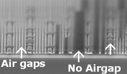
However, the company disclosed that for the tightest-pitch interconnect layer (56nm for both lines and spaces) on 32nm node test chips (see figure), a >20% reduction in the effective capacitance was achieved with air-gaps. Moreover, the company claims that 22nm node test chips show ~28% capacitance reduction compared to full SiOC(H). While the specific dielectrics used were not disclosed, from known films we can guess likely scenarios. The pinch-off dielectric is almost certainly SiOC(H), since any other stable material would have k>3 and would increase the effective k too much. The conformal CVD film could be SiOC(H), or SiO2, or even SiC since the k value of a liner would add relatively little to the final effective k.
The lithographic masking step is needed for two reliability reasons. First, by excluding air-gap formation in areas near next-layer vias, alignment between layers can be more easily done. Second, wide spaces are excluded where the final non-conformal CVD step wouldn’t automatically pinch-off to close the gaps; leaving full SiOC(H) in wider spaces also helps with mechanical strength. The next layer is patterned with a conventional daul-damascene flow, with the option to add air-gaps.
With the masking step to improve reliability and lifetime (see figure), and with etch and deposition optimization, Intel claims that air-gap pilot manufacturing yield for 32nm SRAM tightest-pitch layers is similar to the process-of-record (POR). The company tested dielectric breakdown and thermo-mechanical packaging issues with various air-gap integration flows, and found that the proper combination of barrier layers allowed for equivalent results to the POR. The quality of the interface between the conformal CVD dielectric and the metal is important. Also, the quality of the metal barrier must be good to eliminate fast diffusion paths that could induce unacceptable levels of electromigration.
Perhaps the most significant claim of this new interconnect process flow is that no new failure modes were reportedly observed. In contrast, PLK process flows to get to >10% porosity use new materials and new process steps that almost always combine to produce new ways for the integration to fail, which is another reason that PLK dielectrics have so far failed to replace SiOC(H).
Remembering that Intel is the company that Andy Grove built, and that Grove wrote the book entitled “Only the paranoid survive,” it remains reasonable to consider mildly paranoid theories about the company’s motives. In particular, history has shown that next generation technology announcments can sometimes be deliberate mis-directions: publishing detailed maps that just happen to omit known dead-ends. Intel has not said it will ever use air-gaps in production. All the company has said is that it could use air-gaps in production with good results. Since it is the only known IC company with 1D logic designs ready to go, it could happen for 22nm node manufacturing.
Thorough coverage of IITC this year has been provided by industry expert and Techcet analyst Mike Fury, who attended the full conference including the short-course. Fury’s wit often equals his wisdom, even if he has pony-tail envy. –E.K.
Tags: 22nm, 32nm, air-gap, Cu, IC, integration, interconnect, logic, low-k, materials


