Monday, July 19th, 2010
Two of the biggest original equipment manufacturers (OEM) supplying semiconductor fabs have released new etch chambers that are tuned for the selective removal of mere monolayers. Applied Materials just announced a new “Mesa” field-retrofittable upgrade to it’s “AdvantEdge” ICP etch chamber, targeting several challenging new applications. Tokyo Electron provided an update to applications plans for the Radial Line Slot Antenna (RLSA) chamber first announced in March of this year. Both tools have reportedly passed
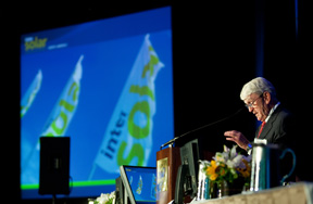
beta-site tests, as this editor mentioned in his invited talk at the NCCAVS Plasma Applications Group meeting, held July 15 this year on the floor of SEMICON/West-Intersolar (figure).
Single-wafer etch chambers have historically been designed for maximum etch rates to deal with microns of material, starting from the first etcher released in 1979 by Tegal (still supplying tools {Thanks to Tegal vice president Paul Werbaneth for the invitation to present at the NCCAVS-PAG}).
From the 1981 release of the Lam AutoEtch 480—featuring atmospheric loadlocks and fully automated recipe control—to today’s tools handling 45nm CDs, maximum etch rate has always led to greater throughput and thus to better Cost-of-Ownership (CoO). However, for 45nm node and below ICs, Dennard Scaling in support of Moore’s Law has led us to device structures where critical materials are now measured in terms of monolayers. The result is an opening in the market for process chambers that are specifically designed to etch as little as a single layer of atoms across 300mm wafers.
However, we are specifically not considering the use of true atomic-layer etch (ALE)—conceptually similar to atomic-layer deposition (ALD) where reactants first adsorb then react and byproducts somehow finally sublimate—for chip manufacturing yet. Nor are we considering the use of neutral ion-beams which can remove atomic layers but generally lack selectivity to underlying materials. At present, it seems that we only need to extend legacy etch chambers with new sources and recipes to be able to meet current needs. How needy are we these days?
 Perhaps the most challenging etch need today is for high-k metal-gate (HKMG) transistors used in 45nm and below CMOS ICs, where work-function altering oxides of aluminum and lanthanum are less than 1 nm thick. Since the gate is the heart of the transistor, any variation in etch profile across the wafer directly results in final device variability, and so as a rule of thumb we must control the etch to 10% of thickness…less than a single atom.
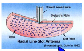
Originally developed for satellite broadcasting, RLSA has been explored as a plasma source by Tokyo Electron for many years (figure). Work at the Tokyo Electron Technology Development Institute in Hyogo, Japan has been led by vice president and general manager Tosh Nozawa. In an exclusive interview with BetaSights, Nozawa-san explained that the 2.45 GHz RLSA source demonstrates the unique ability to provide uniform etching across an extraordinarily wide pressure range: from 5 mT up to 5T.
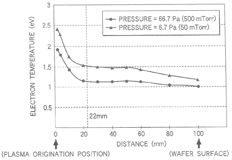
RLSA etching provides relatively high densities of radicals decoupled from the electron temperature (figure). The wafer is not completely “downstream” from the plasma, so anisotropy can be maintained with bias. However, the electron temperature can be as low as 1 eV at the wafer surface, and TEL reports minimal charging damage on sensitive test structures compared to legacy sources.
Applied Materials has found a way to extend a legacy inductively-coupled plasma (ICP) source with two complementary techniques: additional source-coil complexity, and an innovative way to synchronize pulses to both the source and bias powers. Standard ICP source coils have been split in two, which allows for cross-chamber tuning of the electric field (figure). The result is better control of etch rate over the 300mm wafer surface, and the ability to fine tune within-wafer uniformity.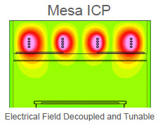
More innovative is the new source-bias sync (figure) that provides superior within-die uniformity. When power is off during the cycle, there are several significant local uniformity benefits:
- charging on the etch mask has time to dissipate,
- byproducts inside recesses have time to exit, and
- reactants have time to refresh surfaces inside recesses.
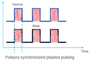 Also, the duty cycle can be adjusted to seriously slow down the process to handle monolayers. “For example, the etch rate can be tuned down to one Angstrom/minute using chlorine plasma,” claimed Thornsten Lill, Applied Materials’ vice president of etch technology development, in an exclusive interview with BetaSights. Compared to a continuous-wave plasma that over-etches 4nm, the synchronous pulsing over-etches <1nm.
Applied Materials reports that the combination of the split ICP source with source-bias-sync significantly improves the depth uniformity when there is no etch-stop, such as in shallow-trench isolation (STI) and buried word-line (bWL) etches into silicon. The company claims 1% silicon etch-depth can be maintained across 300mm wafers, and <1 nm (3 sigma) CD for lines/spaces. Where the use of a continuous wave source would result in measurable non-uniformity in etching trenches, the pulsing source reduces the non-uniformity by 2/3.
TEL has provided the forward-looking-statement that 20 chambers are expected to be sold in the first year, for applications in both transistor and interconnect formation. Applied Materials has provided the backward-looking statement that it has shipped >60 chambers over the last 6 months to etch both metals and silicon, and that the hardware changes can be field-retrofitted in a single production shift. Based purely on end-user demand, it is likely that other OEMs will release new or significantly upgraded plasma etch chambers, and the market for soft plasma etchers will be very dynamic for the next few years. “The more selectivity you have in the etch the more flexibility you have in the overall integration,” said Uday Mitra, Applied Materials’ vice president and chief technical officer of etch, in an exclusive interview with BetaSights. For process development and integration, these new etch capabilities are very welcome additions to the metaphorical tool-box. –E.K.
Tags: 22nm, 32nm, 45nm, ALD, ALE, CMOS, CoO, Denard, etch, HKMG, IC, plasma

