Wednesday, January 14th, 2009
Smart Equipment Technology (S.E.T.), a wholly-owned subsidiary of Replisaurus Technologies and a leading supplier of high accuracy die-to-die (D2D), die-to-wafer (D2W) bonding and nanoimprint lithography solutions, announced yesterday that it will collaborate with IMEC on 3DIC R&D. IMEC’s 3D integration program explores 3D technology and design for applications in various domains, focusing on 3D WLP and 3D stacked-ICs to find innovative solutions for the cost-effective use of 3D interconnects.
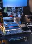
S.E.T.’s automated FC300 flip chip bonder will be used in the joint development program to work on die pick-and-place and bonding processes for 3D chip integration. With more than 250 tools installed worldwide, from semi-automated for R&D through automated for production, S.E.T. bonders flip both fragile and small chips onto substrates up to 300 mm. The FC300 is spec’d with accuracy of 0.5µm, and capable of applying high force (4,000N).
The program is scheduled to begin during the first quarter of 2009, at which time S.E.T. will enter IMEC’s Industrial Affiliation Program (IIAP) on 3D integration. The parties will collaborate to develop both pick-and-place and bonding processes, which are required by advanced 3D integration schemes. “The Replisaurus and S.E.T. technologies are very interesting for advanced packaging applications, and the integration of this tool in particular will help complete our program,” said Luc van den Hove, Executive Vice President and COO of IMEC.
“IMEC’s installation of the FC300 is fully in line with Replisaurus’ product and technology portfolio, which offers game-changing opportunities to the global chip market,” said James Quinn, CEO of Replisaurus. Replisaurus is selling a tool to do ElectroChemical Pattern Replication (ECPR) for integrated passives, copper pillars and TSV. When I met Quinn two years ago, his vision was to develop the full infrastructure needed to bring ECPR to production. Phil Garrou provides an excellent overview of ECPR in his recent blog at SI. While this process is still in beta evaluation, the principle of low-cost micron-scale (instead of nm-scale) patterning is unquestionably the right solution for advanced packaging. –E.K.
Tags: 3D, bonder, chip, ECPR, flip-chip, IC, integration, interconnect, JDP, stacked

