Thursday, August 5th, 2010
Steady but undramatic progress was the theme of lithography presentations at SEMICON/West this year, not that anything more had been expected. In fact, most of the main lithography companies had decided to give the show a miss this year. TEL was the one company that had a full-scale booth, and there was a process to sell: pitch quartering! According to Masayuki Tomoyasu, chief engineer of overseas process development, TEL has a suite of equipment to fabricate 11nm half-pitch (HP) patterns in a cost effective way. Doing 22nm, the next step in Moore’s Law, would only take half the effort. Improved double-patterning results were also revealed by IMEC/ASML and by Nikon.
TEL’s resist core transfer process is a variation on self-aligned sidewall double patterning, where a “core” is fabricated by standard 193nm immersion lithography, trimmed and etched, then gets coated with a sidewall material (which becomes the circuit pattern) and is finally removed. However, the TEL sidewall material is ALD SiO2, deposited at low temperature on the resist itself, before any etching into a transfer layer.
So, after a wafer with a 40nm half-pitch resist pattern comes out of a coat-develop track, the resist and BARC (and maybe a sacrificial layer) are trimmed to 20nm CD in a TEL Tactras Vigus etcher and then conformally coated with SiO2 at low temperature in a TEL Telindy Plus ALD system (figure). The Tactras Vigus then performs an etch-back on the SiO2 film to open the core, etches and strips out the resist/BARC, and transfers the sidewall pattern into the hard-mask. A post-etch clean in an asher completes the process, leaving a 20nm HP grating. According to Tomoyasu, TEL showed SEMs of its own internal 300mm wafer results, not those of a customer.
To get to 11nm, the process begins at 44nm HP, and uses the ALD SiO2 flow described above—on either the photoresist or an underlying core material—to get to 22nm HP structures. Then another ALD of SiO2 forms new sidewalls. Finally, another multistep plasma etch process opens the tops of the conformal sidewall, removes the cores and etches the second sidewall pattern into the hard-mask. A final clean leaves an 11nm HP line-space pattern on the wafer. Edge-on SEMs showed >3:1 aspect ratios with near 90 degree profiles and good regularity. Any such multi-step process needs to be validated with extensive CD metrology and statistics, but these results indicate that 11nm is no longer a fantasy…if one can pay for 3 etches and two depositions!
Designing for double-patterning
Of course, any layout has to be drawn before it is quartered. Designing layouts that can be fabricated by such “lost-core” techniques is a challenge, but no more so than any other feasible litho method below ~65nm CD. At the Advanced Lithography Symposium held July 14 at the North Hall TechXPOT, Jongwook Kye of Global Foundries described the Design-Technology Co-Optimization (DTCO) necessary for today’s circuit scaling.
According to Kye, his “transdisciplinary” optimization is not a new idea: designers have been trying to accommodate process realities since 90nm when poly went unidirectional. Interdisciplinary communication has just produced more restrictions. At 65nm the active layer became unidirectional, and at 45nm the contact landing pads went away and poly CD became uniform. Double patterning first appeared at 32nm and now we are looking at 22nm. Interdisciplinary collaboration has become essential because the litho process choice and the decomposition for double patterning will become chip- and layer- dependent, with no single optimum method.
Don’t forget old fashioned immersion

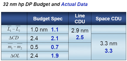
DP budget and actual results achieved with a Nikon NSR 620D immersion stepper. (source: Nikon Precision)
At the Sokudo Litho Breakfast (ably blogged about by Toppan Photomask’s chief technology officer Franklin Kalk), Steve Renwick of Nikon predicted that process development for EUV high volume manufacturing would be delayed until 2015 due to infrastructure issues, and thus the semiconductor industry will need a bridge technology. That technology would have to leverage today’s 193nm immersion exposure tools with double patterning flows.
Source mask-optimization (SMO) with single exposure can give better process windows, but not sub-80nm pitch resolution. So, to get to 32nm HP and beyond, one needs control of CD and image placement. Renwick claimed that the Nikon NSR-620D has met the requirements for 32nm HP (figure) and also demonstrated 20nm HP lines and spaces.
IMEC, the Belgian R&D consortium, separately announced the double patterning results obtained with an ASML XT:1900i immersion stepper equipped with a FlexRay freeform illuminator (figure). Optimized freeform illumination approaches the limits of immersion lithography in geometries where traditional illumination modes cannot. The FlexRay uses a programmable array of thousands of individually adjustable micro-mirrors to create any pupil shape in a matter of minutes (see BetaSights’ exclusive prior coverage of ASML’s “Holistic Lithography”).

Comparison of ASML illumination sources for double patterning of a contact layer along with the images produced, and a table comparing exposure latitude (EL), depth of focus (DOF) and mask error enhancement factor (MEEF). The final hard-mask pattern is at right. (source: IMEC)
The demonstration announced was the contact and metal layer for a 22nm node SRAM of 0.078µm² bit cell area done by LELE double patterning into a hard mask, with the application of simultaneous source – mask optimization (SMO) and FlexRay illumination. The asymmetric X Y positions of the freeform poles cannot be mimicked in a standard source, but would require a custom diffractive optical element likely requiring weeks to deliver.
Stay tuned for a future blog posting about recent EUV, EbDW, and NIL developments.—M.D.L.

