Tuesday, August 17th, 2010
While “Sturtevant’s Law” (which states that optical lithography can make all the circuit structures needed for the next 7-10 years) still may apply, the real limits to any manufacturing technology are financial, not technical. The multiple patterning techniques contemplated for fabricating the next nodes are approaching financial unfeasibility (see BetaBlog post “Steady as she goes: Optical Lithography”). Ten years will take us to the 11nm node or beyond. To deal with this impending disconnect, the industry has been investing in various post-optical lithography schemes including extreme ultra-violet (EUV) illumination, e-beam direct write (EbDW), and nano-imprint lithography (NIL). Progress was reported for all these methods at SEMICON/West 2010, but none seemed about to triumph.
ASML getting ready for HVM with EUV
The leading candidate for next-node patterning continues to be EUV lithography (EUVL) using 13.5nm radiation. Hans Meiling of ASML reviewed the company’s extensive progress towards high volume manufacturing with the NXE:3100 EUVL system and follow-on designs. There are three of these NA=0.25 tools already built at ASML and 3 more being assembled. The first laser produced plasma light source has been attached to a 3100 exposure tool and “first light” (slit exposure) achieved.
Exposure power is 20W now, but a path has been defined for a 5X upgrade. The collector performance was reported as stable. While an NA=0.25 will likely have resolution sufficient to print ~27nm chips, getting to 22nm and beyond will require higher NA and some resolution enhancement trickery.
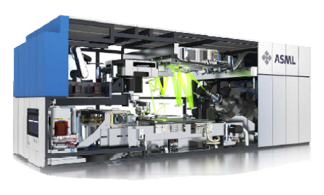
Thus ASML has begun work on the NXE:3300 series (figure), which will feature a 0.32 NA projection system and off-axis illumination capability. The NXE:3300B is scheduled for release early in 2012 and is targeted for 125wph throughput. However, achieving that will require a source 12X more powerful than has been demonstrated, Meiling concedes.
Direct Write Alternative
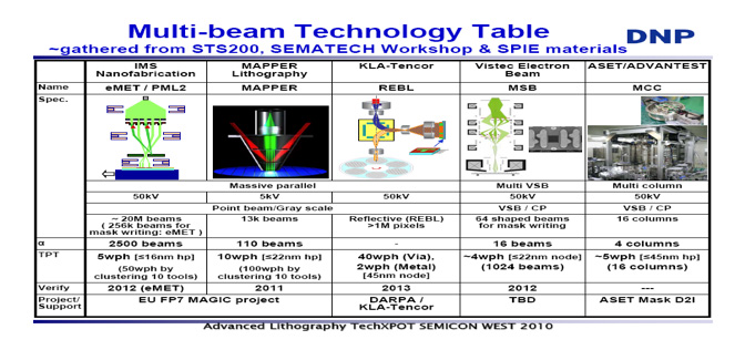
E-beam Direct Write (EbDW) lithography would appear to be a solution to the resolution limit of immersion steppers and the throughput limits of EUV, but the throughput of foreseen EbDW installations is still seen as hideously low. Laurent Pain of CEA-Leti reviewed the progress made by two European efforts: PL2 at IMS in Austria, and Mapper in the Netherlands. Three other programs exist elsewhere (figure).
PL2 operates at 50kV and 200X demagnification and has demonstrated 25nm half pitch. The aperture plate in today’s prototype produces 2500 individual beams, of which 90% work properly, according to Pain. Still, getting 6 wph throughput would require an installation with 76 e-beam columns (one for each exposure field) and 256,000 beams per column.
Mapper would require only 13,000 beams at 5kV, but the present prototypes operate only 110 beams…with a throughput of 0.002wph. Going to 10wph requires getting all the beams to work and raising the beam current 40X. If that could be achieved, a cluster of 10 Mappers would use less floor-space than an EUV tool and yield 100 wph. Most likely, though, EbDW would be used first for the line-cut lithography in a spacer multiple patterning scheme since the duty factor would be low, speeding throughput for the <22m cuts.
Mask making gets some attention
The mask making industry stands to benefit from developments in EbDR, according to Naoya Hayashi of DNP, since a workable wafer writing tool can be modified to write 4X masks with little difficulty. However, mask writing is no longer the cost driver or throughput gate for mask-making. Rather, inspection has taken over as the time-sink and largest expense.
Hayashi predicted that optical lithography (with very complex patterns) will likely continue to dominate for logic chip production, but other technologies like EUVL and imprint will pose different and unique challenges for mask makers if they are adopted by some industry segment. Developing the proper tool sets and processes in time will be a challenge for mask makers if there is no industry consensus. Hayashi suggested that device manufacturers and tool vendors should include mask makers in collaborations to find workable next-generation patterning solutions.
Imprint pressing on
The only pattern transfer technology that will avoid design restrictions at 11nm is imprint, according to Ben Eynon of Molecular Imprints Inc., who also predicted that NIL’s cost of ownership will be independent of resolution! MII is overcoming the limitations of its J-FIL technology and Eynon expects to see memory production with it ramp in 2012 or 2013. Defectivity is now <1/cm2 in a clean-room environment, according to Eynon, and mix-and-match overlay <12nm has been achieved using template squeezing with force sensor feedback.
NIL infrastructure issues were being addressed: E-beam inspection and repair tools for the 1X master templates exist as does a capable cleaning tool. Master masks can be written slowly today at 14nm resolution with a 100kVGaussian E-beam tool, but a faster vector-scan will do 22nm. The master masks are being replicated with <20nm half pitch in MII’s TR1100 template production system. With replication, the cost of production with imprint is ¼ that of immersion double patterning and ½ the projected cost of EUV, according to Eynon. The first MII 5XX series pre-production lithography system was shipped in July.
In 2005, Ken Rygler (then the chief marketing officer of MII) bet Brian Grenon that 193nm exposure would be used for 22nm node production, with Grenon betting that something else would be needed, possibly imprint. The time is coming to find out who was right. That the issue is not already decided is a testament to the cleverness of the optical lithography community and the difficulty of every post optical alternative.—M.D.L.
Tags: 193, 193i, 22nm, 32nm, cost, DP, EbDW, EUV, IC, litho, mask, NIL


