Tuesday, September 14th, 2010
Electron-beam (e-beam) lithography has long printed the photomasks used for chip production, but conventional vector-scanned e-beam tools will take too long to write the highly complex structures needed for the 22nm node if they have to be exposed using 193nm immersion (193i) lithography. That puts mask-makers in the same bind as chip-makers who have craved higher throughput in e-beam direct write (EbDW) lithography. Now, some of the innovations developed for direct write chip production are being applied to mask-making, as revealed at the SPIE/BACUS Photomask Symposium, today in Monterey, California.
 The trick, according to Aki Fujimura, CEO of D2S and managing sponsor of the e-Beam Initiative (figure), is design for e-beam (DFEB) along with cell projection e-beam exposure tools. In the cell projection, the e-beam column is equipped with shaped apertures that match typical wafer or mask geometries so that they can be printed in a single shot, rather than assembled from the rectangular shots of a conventional vector-scanned e-beam mask writer. DFEB encourages layouts that employ these pre-defined shapes to reduce the number of exposures needed for a mask or wafer. Using both methods can reduce the time needed to write a 22nm-node mask from ~80 to <30 hours, according to Fujimura. “The more complicated the mask is, the more we can help,” he stated in a pre-conference interview on Sept. 7.
The masks have gotten so difficult to produce because they have to be designed for manufacturing with 193i exposure tools, which have an intrinsic resolution limit of ~40nm. Obtaining an acceptable process window for features that size requires adding curvilinear sub-resolution assist features (SRAF) to the mask. The end result is that the 4X mask pattern becomes much more complicated than the chip, with minimum features of similar size. Applying DFEB to DFM masks is something of a revolution as it forces designers to confront yet another real-world manufacturing limitation.
The good news, according to Fujimura, is that DFEB can reduce the complexity of mask making by applying knowledge of the e-beam exposure process. Near the resolution limit of an e-beam exposure tool, the resist patterns are rounded and the exposures graded at the edge, just as they would be in optical lithography. Understanding the dynamics of e-beam exposure allows model-based fracturing with shapes overlapping rather than adjacent. Modulating the dose reduces the roughness of the edges without increasing the shot count. The net effect is faster throughput with better mask functionality, averred Fujimura.

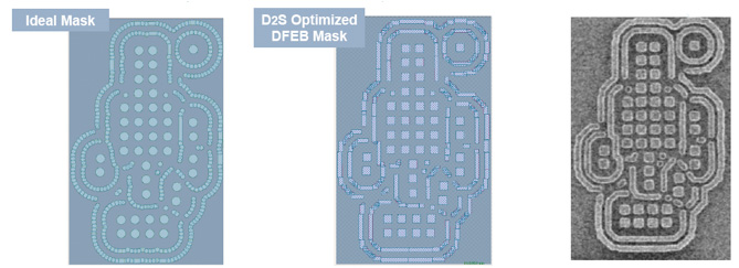
An ideal ILT mask layout for a contact array fractured for printing mostly with circular beam spots and a DFEB optimized layout with fewer shots, finally an SEM of the resulting resist pattern on the mask. The contacts are meant to print at ~55nm diameter. (source: The e-Beam Initiative and JEOL)
Some of the advantages of DFEB mask technology had been presented at the 2010 Photomask Japan conference in April. Jeol has developed the JBL 3200MV, a mask writer with circular apertures to print round shapes and the capability to vary dose. The first example of an inverse lithography 22nm node pattern written with that tool showed a 30% shot reduction compared to a manhattanized fracturing and VSB exposure and showed better CDU (figure). At BACUS, the e-Beam Initiative reported another 17% shot reduction when DFEB methods had been applied to a manhattanized layout and printed with conventional VSB shapes. The net result is a 40% reduction in write time.
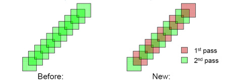
AIMS analysis showed the ideal and DFEB rectangular masks were functionally equivalent. Further throughput enhancement were predicted with dose modulation (figure); a curvilinear SRAF can be printed in two passes if each shot has ½ the dose, or with every other shot at full dose. That would reduce beam blanking time by 50% and speeds SRAF writing by 25%.
DFEB for masks speeds the printing of sub-30nm layouts that were previously unfeasibly complex. However, there is more to semiconductor mask-making than e-beam writing. Chips have to be designed, modeled, laid out, design rule checked, taped out, fractured, mask rule checked, written, inspected, re-written, and repaired… and then the mask set has to be accepted by the customer. The e-Beam Initiative is seeking buy-in from all participants in this complex ecosystem. All have secrets to keep. On September 7, 2010, the Initiative announced that 4 new player have joined the prior 30: Abeam Technologies, EQUIcon Software GmbH Jena, Synopsys, and TOOL Corporation.
The e-Beam Initiative has a considerable educational task ahead of itself if it is going to succeed in introducing DFEB masks at the 22nm logic node (HVM in 2012 or 2015). Fujimura reported that collaborative development is on-going now, with only a part being reported in the four papers presented at BACUS. Since no one can keep a mask writer working properly for 80 hours, one has to wish them well. – M.D.L.
Tags: 193i, 22nm, 32nm, BACUS, CDU, D2S, DFM, e-Beam Initiative, EbDW, IC, Intel, litho, mask, node, SPIE, SRAF

