Thursday, September 23rd, 2010
Through-silicon vias (TSV) have been in R&D for over 10 years, and finally may reach commercial use in IC manufacturing next year. However, instead of forming vias through silicon in ICs (TSV-IC), the near-term needs will be for vias though silicon interposers (TSV-interposer) made in outsourced test assembly and packaging (OTAP) fabs. Presentations at conferences including SEMICON/West, IMAPS, and IEDM in this year provide perspective on the slow evolution of this 3D IC technology.
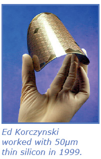
 TSV has been a bit of a “solution looking for a problem” since first conceived. This editor worked on the technology in the years 1999-2000 for a startup called TruSi (now a TSV-interposer foundry called AllVia, to which this editor has no relationship), trying to sell an atmospheric pressure etch tool to do silicon thinning to 50µm (figure) and below. Despite continued interest in TSV capabilities, a viable (pun intended) “problem” was always lacking. Nonetheless, the entire industry ecosystem of original equipment manufacturers (OEM), specialty materials suppliers (SMS), and consortia have continued to develop and push TSV technologies out into the world. In addition, there have always been “boutique” mil/aero companies like Vertical Circuits with 3D-IC IP looking to expand into high-volume commercial markets. The result is a confusion of options, and no real cost or yield data for volume manufacturing.
Perpetual pundit Phil Garrou—now blogging for PennWell’s “ElectroIQ” site after being tossed out with other editors when Reed closed Semiconductor International—reports that leading OSAT ASE is soon going to be ready with TSV-interposers. During OEM Suss Microtec‘s “3D IC Bonding and Thinned Wafer Handling Workshop,” at SEMICON/West this year, Calvin Cheung, vice president of engineering for ASE, said, “We currently need an interposer to bond 28nm low-k die,” he said. “Right now it is impossible to stack these mechanically unstable materials into a reliable 3D stack in any other way.”
Alchimer also held a workshop at SEMICON/West to show how it’s all-wet molecular deposition technology can reduce costs in any TSV fill step. During this workshop, Riko Radojcic, director of engineering at Qualcomm CDMA Technologies, said that, “We have certain form-factor constraints that may motivate us to use TSV.” The killer-app is video processing bandwidth in mobile devices, and, “if it will be 3D based on TSV or PoP remains to be seen…but it’s clearly not going to be served by routing through a PCB,” said Radojcic. For Qualcomm’s 3D circuits, the logic chip would be on the bottom with TSV-IC, while memory or analog would be on top as a flip-chip. “We focus on heterogeneous integration,” explained Radojcic, “not logic on logic stacking.” Qualcomm’s 3D stacks already have to manage power for other reasons, so any eventual TSV-IC would not need thermal vias.
The IMAPS 2010 conference scheduled for November 2-4 this year in Raleigh, North Carolina will include a special track on 3D packaging and integration [NOTE: early registration and hotel deadline Sept. 24]. One presentation will be on “Enabling robust copper fill of super high aspect ratio through silicon vias” by Novellus Systems. In an exclusive interview with BetaSights, Novellus’ senior director of business development for 3D applications Damo Srinivas confirmed that interposers appear to be the main near-term TSV volume, and so the final silicon target thickness will be 100-140µm.
Interposer thickness cannot be reduced below 100 microns without rigid silicon wafers becoming flexible silicon foils. Typical TSV processes to date have worked with 5:1 to 10:1 AR, which may be acceptable for TSV-IC that could be 10-50µm thick. However, 10-20µm diameter TSV consume too much silicon area, and take too long to etch and fill. Novellus has integrated a low-temperature vapor deposited dielectric, Cu barrier/seed vapor deposition, Cu electroplating, and Cu overburden wet-etchback in 20:1 AR TSV 100µm deep. Novellus has also claimed that proper integration of the barrier/seed and ECD steps allows for control of the Cu grain orientation inside TSV, such that post-anneal protrusion can be reduced from 0.8 to 0.2 µm, and at IEDM 2008 protrusion was shown by IBM to increase contact resistance.
TechSearch International has recently published a market forecast for silicon interposers, as part of the company’s Advanced Packaging Update Service.
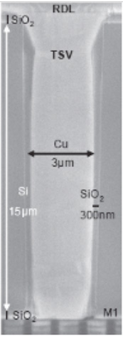
- Some day the world will probably need TSV-IC for mainstream commercial chips. To that end, the 56th International Electron Devices Meeting (IEDM 2010) in San Francisco, California, December 6-8, will include a presentation on TSV-IC titled, “Investigation on TSV impact on 65nm CMOS devices and circuits.” French researchers put 4µm diameter TSV through 65nm node ICs (figure), and for the first time experimentally quantified an electrical coupling between TSVs and MOSFETs. This coupling induced a spike variation of up to 7 µA/µm on the static NMOS drain current, though ring oscillators nearby were reportedly not effected. –E.K.
Tags: 3D, ASE, Cu, ECD, etch, IC, IEDM, IMAPS, Novellus, OTAP, PVD, Qualcomm, TSV

