Monday, November 8th, 2010
Xilinx has found the first major commercial IC fab problem which through-silicon vias (TSV) can solve: barrier-to-entry for large FPGAs and pseudo-SoC chips. BetaSights recently covered TSV technology pushed as a “solution looking for a problem,” and forecast use of TSV in silicon-interposers (“2.5D”) as the only significant near-term commercial volume. Ed Sperling at Chip Design recently covered TSV technology pulled as part of 3D stacking for 28nm and below chips. For Xilinx’s 28nm node Vertex-7 product, TSMC will use a 65nm node fab line to form TSV in silicon interposers along with multi-level-metal (MLM) interconnects.

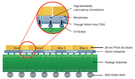
Xilinx uses passive silicon-based interposers, microbumps, and through-silicon vias (TSV) for its 28nm node 7-series FPGAs (Source: Xilinx)
The device is made using micro-bump assembly and a special FPGA architecture to match the interposers (figure). The multi-chip device delivers lower levels of power consumption, system cost, and circuit board complexity compared to using multiple FPGAs, each in their own package, for the same application. “Compared with traditional monolithic FPGAs, multi-chip packaging approach is an innovative way to deliver large-scale programmability with favorable yield, reliability, thermal gradient, and stress tolerance characteristics,” said Shang-yi Chiang, senior vice president of R&D at TSMC. Specs include up to 2.4Terabits/sec I/O bandwidth and 4.7 TMACS DSP performance.
Data flows between the FPGA dice and the interposer through more than 10,000 routing connections, providing over 100X the die-to-die connectivity bandwidth per watt at one-fifth the latency compared to prior multi-chip packages, without consuming any high-speed serial or parallel I/O resources. Xilinx claims that TSMC’s 28nm HPL (high-performance, low-power) process technology for the base FPGA device provides a comfortable power budget in the package.
Xilinx positions the 2 million logic cells possible in the device as extending the range of applications which can be addressed by an FPGA. “Our stacked silicon interconnect packaging approach makes this remarkable achievement possible,” said Vincent Tong, Xilinx senior vice president. “Five years of Xilinx research and development coupled with industry leading technology from TSMC and our assembly suppliers has made possible our efforts to provide an innovative solution…” The device targets next generation 100GE line cards, 300G bridges, Terabit switch fabric, 100G OTN muxponder, RADAR, and ASIC emulation.
Integration benefits of TSV interposers
“The Virtex-7 2000T FPGA using stacked silicon interconnect technology is a significant step in FPGA evolution and will enable ARM to implement the latest cores and platform solutions within a single FPGA. This will reduce our development effort, reduce power, and improve performance compared to a multi-FPGA approach,” said John Cornish, EVP and general manager, System Design Division, ARM. “We have been a long time user of the Virtex FPGA technology in the ARM Versatile Express SoC prototyping solutions and this will surely extend our strong position.”
Not specified by Xilinx but generally known is that silicon-interposers easily incorporate passive circuit elements such as resistors, capacitors, and inductors. If you have already committed to the integration expense of interposers for other reasons, then you almost certainly will want to take advantage of ability to integrate passives. All Silicon Systems Integration Dresden (ASSID) program within Fraunhofer IZM works on Cu-TSVs with diameters in the 2-20 ?m range, and on functionality extensions of 300mm silicon interposers with passives. Rolf Aschenbrenner (figure) has recently been appointed as the deputy head of Fraunhofer IZM, and co-head of the Systems Integration and Interconnect Technologies department.
Time-to-market for both large FPGAs and FPGA-based SoCs should be improved by the use of TSV-interposers. Xilinx claims it was challenged by some of it’s customers to be able to supply high-volumes of 2M-gate FPGAs almost immediately after the start of production, when line yields are still low. Modeling showed that early line defect levels would kill most 2M-gate chips but most 0.5M-gate chips would yield, so combining four of the latter using a high-bandwidth silicon-interposer will allow the functionality to reach market much faster. Xilinx is now proving software design support to beta customers, and initial devices will be available in the 2nd half of 2011.
Vertex-7 designs are available as part of “EasyPath-7” software, allowing portability to lower cost while lower performing FPGA families. The Artix-7 family–optimized for lowest power and lowest cost using wire-bond chip-scale BGA packaging–addresses cost-sensitive, high-volume markets like portable ultrasound, digital camera control, and software defined radio. The Kintex-7 family– optimized for low power signal processing using BlockRAM and DSP–is for wireless LTE infrastructure equipment, LED backlit and 3D digital video displays, medical imaging, and avionics imaging systems.
On November 16, the San Francisco Bay Area (SFBA) Nanotechnology Council Chapter of the IEEE is hosting a ½-day symposium next week on “Nanoelectronics: Innovation and Implementation” that will include a presentation by TSMC vice president of technology applications Di Ma on “Technology Challenges in 28nm CMOS and Beyond.” GloFo and Samsung will also give presentations at the event, which will be held on National Semiconductor’s campus in Santa Clara. Stay tuned for more news on 2.5D ICs. –E.K.
Tags: 22nm, 28nm, 32nm, ARM, ASSID, Cu, FPGA, IC, IEEE, integration, interposer, IZM, MLM, Si, SoC, TSMC, TSV, Xilinx, yield

