Tuesday, December 21st, 2010
Graphene—the 2D hexagonal lattice of carbon—has been under investigation as a new material for electronics applications due to it’s high mobility and other unique properties. At IEDM this year, an entire session (#23) was devoted to showcasing graphene devices, and to sharing the latest processing tricks to grow and (sometimes) transfer the single-atomic-layer of carbon to an oxidized silicon wafer. High-speed analogue (RF) circuits have been shown by IBM, SAIT, and MIT, and IBM has created a 130 meV bandgap with ~400 meV predicted as possible. Outside of IEDM, GeorgiaTech has published on how to form 10,000 top-gated graphene transistors in 0.24 cm2 of SiC chip area.
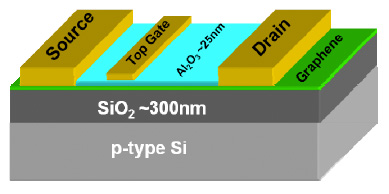
IBM researchers in Yorktown Heights, NY (S23P01) presented an invited paper on graphene applications, including discussion of how to form a bandgap in bilayer structures that allows for the creation of optoelectronic devices and possibly even digital circuitry (figure). These bilayers have a four atom unit cell, hyperbolic dispersion, and no intrinsic bandgap. However, the application of a strong perpendicular electric field produces an asymmetry by inducing charge transfer between the layers.
Using dual-gated (top and bottom) graphene field-effect transistors (GFET) with an NFC/HfO2 gate stack, field-tunable bandgaps of more than 130 meV were created, with on/off ratios of ~100 at room temperature and >1000 at low temperatures. Although this small gap is still not sufficient for digital devices, it could be used in optoelectronic applications such as THz emitters and detectors. With improvements in both the graphene and dielectric quality, a bandgap of ~400 meV has been predicted to be possible.
A sophisticated photodetector can be fabricated using bilayer graphene. Multiple inter-digitated electrodes are made using two metals with different workfunctions: Pd and Ti have been shown. At appropriate backgate biases, the different workfunctions and resulting asymmetric band-bendings generate a sloping overall potential along the graphene channel that allows photodetection over the entire device. This type of device was tested and found to be able to reliably detect optical data streams of 1.55 micron light pusles at a rate of 10 GBits/s (maximum capability of the measurement system) without an applied source-drain bias.
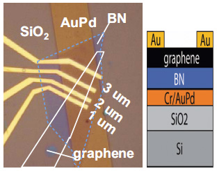
Columbia University researchers (S23P02) used exfoliation of single-crystal hexagonal boron nitride (h-BN) as the gate under exfoliated graphene to create FETs with mobility values exceeding 10,000 cm2/V•sec and current saturation down to 500 nm channel lengths with intrinsic transconductance (gm) values above 400 mS/mm (figure). Because the h-BN can be made arbitrarily thin (down to a single monolayer), the same h-BN dielectric layer can function as both a supporting substrate and the local-gate dielectric. Top ohmic contacts were made using Cr/Au (1nm/90nm), producing p-type doping of the graphene under the contacts because of work-function differences.
Researchers from Seoul National University and Samsung Advanced Institute of Technology (S23P05) reported on a similar graphene layer transfer technique onto oxidized silicon wafers with locally-embedded TiN back-gates to create RF devices. Despite underlap between the gate and the source/drain, researchers measured a record maximum mobility of 9000 cm2/V•s, with a general range of 3000-6000 cm2/V•s which allows for fT =80 GHz using 0.24micron gate lengths.
Despite these high mobilities, gm and Ids still remain low for various reasons associated with the R&D processes used on 150mm diameter wafers. Causes could include high contact resistance due to poor adhesion from lift-off process, impurities between the gate oxide and graphene channel from the graphene transfer, or contamination of the exposed graphene channel under ambient conditions.
MIT researchers discussed (S23P06) how the unique ambipolar transport properties of graphene, combined with its high mobility at room temperature, enable the development of a new form of non-linear electronics for radio frequency (RF) and mixed-signal applications.
Single-layer graphene films can be grown by CVD on sacrificial copper substrates. Firstly, copper foils are annealed at 1000°C in H2 (350 mTorr for 30 minutes) to increase their grain size, then they are exposed to low-pressure (1.6 Torr) CH4 to initiate large poly-crystalline graphene growth (80 x 80 micron plan-view of a single-crystal shown). Next, polymethyl-methacrylate (PMMA) is coated on the graphene film and the copper substrate is etched away. Finally, the graphene is transferred onto polished Si wafers with a 300nm thermally-grown SiO2, where Hall effect measurements show mobilities in the 1800-2500 cm2/V•s range.

MIT's graphene on insulator device formed by layer-transfer from a sacrificial Cu-foil (source: IEDM2010)
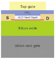
Ohmic contacts are formed by depositing a 2.5nm Ti/45nm Pd/ 15nm Au metal stack by e-beam evaporation. Device isolation is achieved by O2 plasma etching. The gate dielectric consists of 5nm of e-beam evaporated SiO2 as a seed layer, followed by 15nm of ALD Al2O3. The top gate is formed with a 30nm Ni/ 200nm Au/ 50nm Ni metal stack (figure).
For frequencies >400GHz, the presenter mentioned that efficiency is often <20% for today’s frequency multipliers. In stark constast, this graphene device shows the ability to double a 700 MHz input to 1.4GHz output at room temperature with >90% of the output power, and without the need for any filtering elements. The high quality of graphene devices could thus allow for more efficient analogue and mixed-signal circuits, since each filter is a source of noise and loss. Potential security and medical screening applications would use 0.3-10 THz frequencies that can pass through fog, fabrics, plastics, and bricks. Theoretically, graphene devices could be used for power gain, though no one has yet shown such function.
A team from IBM and MIT (S09P06) demonstrated RF performance of sub-100nm graphene transistors fabricated using epitaxial growth on a SiC substrate. A cut-off frequency as high as 170 GHz is achieved in a 90nm graphene FET using NFC/HfO2 as the top gate dielectric, and e-beam evaporating 20nm Pd/30nm Au as the contact metal.

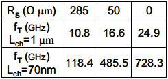
Modeling of gm by varying Rs for 70 nm and 1 ?m devices and the improvement of projected fT. (source: IEDM2010)
Transconductance (gm) can be improved by 4 times for a 70nm device by reducing the contact resistance, which is much greater effect than in the long channel case (figure). A 90nm-gate graphene FET showed a cut-off frequency as high as 170 GHz at a drain voltage of 2.2V. The device performance is limited by the series resistance, including the contact resistance and the access resistance associated with ungated region. Consequently, the researchers model that the cut-off frequency can be enhanced to as high as 350 GHz using a self-aligned gate structure.
Outside of IEDM
Outside of IEDM this year, Georgia Tech folks recently published work in Nature Nanotechnology on the preferential epi growth of graphene nanoribbons on the sidewalls of properly oriented silicon carbide recessesses. Structures are formed using photolithography and etching. Pre-epi, the wafer is heated to ~1,500°C to melt and polish any rough edges left by the etching, so as to avoid electron-scattering. These prototype graphene devices exhibit a weak on:off ratio of 10, with carrier mobilities up to 2,700 cm2/V•s at room temperature. However, while dependent upon SiC as the substrate instead of Si, this approach has already allowed for the fabrication of 10,000 top-gated graphene transistors in 0.24 cm2 of SiC chip area, claimed as the highest density of graphene devices reported to date.
Though all of this is still far away from commercial manufacturing, the fact that epi-growth and layer transfer of graphene has been shown to produce highly functional devices is an indication that we are headed in the right direction. Potential applications have been shown for high-speed analogue circuits and novel light sensors. –E.K.
Tags: analog, analogue, backgate, bandgap, gate, GeorgiaTech, GFET, graphene, HfO2, HK, IBM, IC, IEDM, MIT, mixed-signal, mobility, RF, SAIT, SiC, THz


