Friday, January 23rd, 2009
Researchers from Sungkyunkwan University (SKKU) in Korea have found that large graphene films can be formed using CVD over a Ni thin film. The graphene is both strong and stretchy, and at low temperatures the monolayers transferred to SiO2 substrates show electron mobility >3,700 cm2/Vs implying that the quality is as high as mechanically-cleaved graphene. Other researchers have reported >200,000 cm2/Vs by suspending a single layer ~150 nm above a Si/SiO2 gate electrode, but only as a scientific discovery. The SKKU CVD process, developed with Samsung AIT, is the first public disclosure of a possible engineering approach to manufacturing graphene devices.
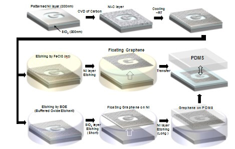
The process flow starts by depositing a 300nm thick Ni layer on a Si wafer. Next, a methane precursor in a CVD chamber at 1000°C followed by a rapid thermal quench forms six to ten atomic layers of graphene. Patterning the Ni layer allows for the creation of patterned graphene for device applications. Two different methods of patterning the films and transferring them to arbitrary substrates have been shown (see Figure).
Prof. Byung Hee Hong, who has been publishing work on manufacturing methods for nanoscale structures since 2001, leads the fabrication work in the chemistry department of SKKU. The lab has the following thin film equipment: e-beam/thermal evaporators, DC/RF PVD, RIE, ion-mill/ICP-etcher, and PECVD and thermal CVD. The crystallographic orientations of the Si wafer and Ni film were not disclosed, but other researcher have reported on the growth of graphene on Pt(111) and TiC(111) surfaces.
Centimeters-wide films that can be bent and stretched without breaking or losing their electrical properties have been shown. The transferred graphene films show very low sheet resistance of ~280 Ohms/square, with ~80% optical transparency. At the upcoming American Physical Society (APS) March Meeting in Pittsburgh, researchers from Purdue University will present information about a condensation technique to form graphene on Ni. Old tricks are being used to create a new material…this all could lead to beta tests of fab processes some day soon. –E.K.
Tags: CVD, electron, film, graphene, IC, mobility, monolayer
