Monday, January 26th, 2009
CEA/Leti, along with e-beam lithography supplier Vistec, and new design and software company D2S, recently announced a collaboration focused on refining and validating advanced design-for-e-beam (DFEB) solutions for 45nm and 32nm nodes. Over the next 12 months, Leti will manufacture test chips using a combination of D2S’ design and software capabilities along with the latest high-resolution e-beam direct-write (EbDW) SB3054 tool from Vistec.
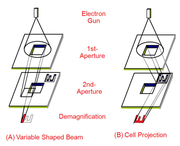
With the cost of advanced mask-sets continuing to increase, direct-write lithography seems essential to allow for low-volume production of custom ICs. EbDW using variable shaped beams (VSB) has been done, but throughput has always been problematic. Character projection (CP) uses standard shapes to convey maximum patterning information in a single e-beam shot. D2S’ software translates the most commonly recurring patterns of chip designs at synthesis into templates on “mini-reticles,” allowing these complex patterns to be replicated in a single CP shot using Vistec’s tool (see Figure). By reducing the design’s required shot count, this approach improves throughput over VSB while enhancing accuracy.
CP itself is obviously a speedup, and making the characters more suitable for the types of designs that might come along can provide a 10-20x increase in writing speed compared to VSB. For a clock-generator or specialized IP there may not be regular characters, but the majority of SoC chips consist of regular blocks like SRAM and I/O that can be made using standard characters. Compared to conventional lithography, assuming $20M/tool for the EbDW tool and 1 wafer/hour writing time and a $4M mask budget, then it is affordable to use CP EbDW for up to 200 wafers according to D2S CEO Aki Fujimura in an exclusive interview with BetaSights.
“If you look at expensive but low-volume products, like high-end cameras or super-computers or FPGAs, if the mask cost can be eliminated and the design-cost is eliminated because it’s a derivative, we can use this technology and serve the long-tail of the market,” explained Fujimura. D2S is also involved in a joint venture with Fujitsu, e-Shuttle, and Advantest, and shuttle runs at Fujitsu for metallization have already started. The work at Leti seems to be focusing more on critical layers. –E.K.

