Wednesday, February 4th, 2009
Allvia, the first through-silicon via (TSV) foundry, has secured $5 million from private investors in a round of funding to expand manufacturing facilities and to build more capacity. After 3 years of revenue generation from providing vertical interconnects and System-in-Package (SiP) solutions, total investment in the company is now $25 million. With in-house processing equipment, a long history of intellectual property (IP) and a fabrication facility in Sunnyvale, California, Allvia offers prototyping services and volume production runs.
TSV are now being designed into many chips, though surprisingly not for the 3D stacking of ICs as many people expected. In an exclusive interview with BetaSights, Allvia CEO Sergey Savastiouk (full disclosure: BetaSights’ Ed Korczynski worked for Savastiouk 10 years ago at TruSi Technologies, but has no current relationship) said that 3D stacking using TSV is not going to happen in mainstream volume anyside soon. Savastiouk mentions issues with reliability, design, and the cost of stacking chips using TSV, and reminds us that it took decades for flip-chip to become mainstream.
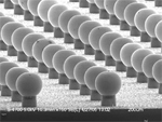
Allvia sees applications for large diameter—defined as >10µm—TSV to be formed using process flows starting from either the backside or frontside depending upon the design. With a portfolio of in-house tools and processes, the foundry can create a wide variety of TSV including dense bumped arrays (see Figure). Allvia is not chasing the elusive market for small diameter TSV targeting 3DICs. “There are two TSV camps today: large and small diameters,” said Savastiouk. “Large is trying to sell today, others are trying to sell into the future.”
Selling today are TSV for image sensors, MEMS, and RF, and most of these count as single-chip and not stacked applications. Passive interposers built with TSV—currently ~1/2 of Allvia’s wafer output—don’t count as 3D stacks and are already in volume production. The company has been active in talking to product people with new devices entering volume production. “There are all kinds of sensors that you have to access from the backside,” explained Savastiouk. Serving a leading technology niche seems like a solid plan. –E.K.
Tags: 3D, foundry, IC, interconnect, MEMS, package, RF, Service, Si, TSV

