Friday, February 6th, 2009
The SEMI PV Group today announced the release of its Global Photovoltaic (PV) Standards Roadmap Guidance Document, which identifies immediate opportunities for reducing cost and accelerating innovation in thin-film and crystalline silicon cell and module manufacturing through industry standards. This new roadmap confirms that major manufacturing cost savings are possible through standardizing wafer carriers and physical interfaces, chemical and gas purity, device tracking, equipment metrics, facilities, safety guidelines, silicon specifications, and process controls.
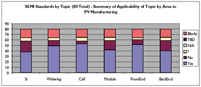
 The Guidance Document provides a high-level assessment of existing SEMI Standards and Safety Guidelines with respect to their applicability to PV manufacturing, as determined by a team of industry stakeholders including equipment and materials suppliers, cell and module manufacturers, and safety experts. Drawing from the 35 years of SEMI International Standards development, over 64 existing SEMI Standards and Safety Guidelines were found that are applicable to PV manufacturing (see Figure). Out of those 64, 31 were rated as ‘Top Priority’ for their potential to deliver immediate cost benefits to the industry with limited or no revisions necessary.
“While many semiconductor equipment, materials, and device manufacturing companies that employ SEMI Standards are diversifying into PV, the PV industry has a highly specialized and unique set of needs, with a diverse set of stakeholders,” said Dan Martin, executive vice president of SEMI PV Business Development and SEMI Global Standards. The Guidance Document further describes planned collaborative initiatives involving other Standards Developing Organizations (SDOs) such as ASTM International, IEEE and others, as well as the increasing participation of research laboratories like NREL (National Renewable Energy Laboratory in the U.S.) and the value of their contributions.
“The next Roadmap development phase will focus on identifying and establishing timelines for the top priority areas in PV manufacturing where new specifications, test methods and safety guidelines will be developed to further reduce the costs of cell and module manufacturing,” said Martin. SEMI is soliciting additional members to join the PV Standards Roadmap Core Team; interested parties should contact Bettina Weiss, senior director, Photovoltaic Segment, SEMI PV Group. –E.K.
Tags: cost, fab, management, PV, Si, solar, standards, thin-film
