Monday, February 9th, 2009
Toshiba claims the prototype of a new Ferroelectric Random Access Memory (FRAM) cell sized at 15F2 acheives read and write speed of 1.6-GB/s using a 130nm node CMOS process. The company will show details of this high bandwidth 128Mb non-volative RAM technology at the International Solid-State Circuits Conference 2009 (ISSCC 2009; Session 27.5) in San Francisco this week. Chips in this family could ultimately be used as the main memory of mobile consumer products, and the cache memory in mobile PCs and SSDs.
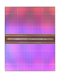
The cell is a re-design of Toshiba’s original chainFeRAM architecture, which was first announced in 2001 as a 30F2 cell of size ~1.9 µm2 using 250nm node technology. Earlier generations of this cell used neighboring data-lines operating in sequence: alternating off lines to provide noise barriers around on lines. By doubling the data-lines at the newer node from four to eight the new cell is just 0.252 µm2, which decreases the total chip area (see Figure). The chip runs on 1.8V, with 83 ns cycle time, and 43 ns access time.
R&D of FRAM technology has been continuous for over 25 years, based on fundamental materials science work on perovskite oxides as the switching layers. It is relatively easy to make a single working FRAM cell in a lab, but it is rather difficult to precisely control the composition of complex trinary oxide thin-films deposited across complex topographies on wafers. Even if you can control the composition properly, the phase can be wrong inside of trenches coated with MOCVD/ALD layers. This is not easy stuff to ramp in a fab.
Chip scaling causes signal degradation as the stored polarization of a memory cell gets smaller. By shortening the data-line pitch in the chain architecture, Toshiba maintained the same cell signal level, and with an improved sensing technique reduced the parasitic capacitance to reach a reading signal of 200mV. Just as parasitic capacitances limit scaling of DRAMs, parasitics limit scaling for FRAMs. The smallest functioning FRAM cell that has been publicized is <10F2, shown by Samsung in 2001, but Samsung’s most recent product announcement in 2002 was for a 32Mb chip using a 0.94 µm2 cell. Some minimal critical mass is needed to hold remnant polarization in useful memory arrays, and so an inherent limit seems to exist for scaling FRAMs. All information on deposition and annealing of switching materials is held secret, so very few people can guess the real scaling limits. –E.K.

