Thursday, February 19th, 2009
JSR announced today that it has entered into several joint development partnerships (JDP) with IBM to develop low-k dielectrics for 32nm and 22nm nodes of semiconductor technology. The companies will work on next generation materials JSR has had in development and commercial production, including low-k dielectrics and a broad range of photoresists. “This larger scale collaboration is a huge complement to the joint research and development JSR Micro is already doing with IBM in photoresist,” said JSR Micro president Eric Johnson.
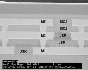
The companies are working to pave the way for the adoption of three new material technologies: CVD low-k, ultra-low-k (“ULK”, a.k.a. “extreme-low-k” or “porous low-k”), and photo-patternable low-k (PPLK), all developed jointly by IBM Research and JSR Corporation. The CVD precursor is based on a novel molecular structure inspired in part by the spin-on ULK work, and reported offers k=2.2 with reduced sidewall plasma damage, better trench bottom roughness, and better CD control over the process of record CVD low-k material. JSR’s current spin-on low-k (see figure) is not included in the JDP.
The ULK is a spin-on which was originally studied by IBM claiming k<2.0 with extraordinary modulus, toughness to CMP, and purported extendability. While these claims are impressive, a single word reminds us that successful betas may end up losing cost battle: “SiLK.” Despite substantial investment by Dow Chemical in the development of SiLK spin-on dielectric resin to support IBM, CVD remains the low-k technology in most fabs. As cost modeled in 1997 (MRS Spring; N3.10; “Cost-per-wafer of various low-k dielectric integration schemes,” Ed Korczynski, Solid State Technology, Campbell, CA), and since conventionally shown, CVD tends to cost less to integrate compared to spin-on which requires additional bake/stabilization steps.
However, a directly-imageable dielectric with near equivalent final integrated material properties would certainly be a huge cost savings over a mere spin-on. This PPLK material, invented by IBM, cuts several sacrificial materials and their related plasma etching steps, saving costs and reducing process complexity. Details of the PPLK technology will be presented at the upcoming MRS and SPIE Advanced Lithography shows in 2009. The SPIE abstract claims k=2.7 integrated into the fat wire levels of Cu-dual-damascene metallization, with “very high electrical yields using the current manufacturing infrastructure.” –E.K.
Tags: 32nm, Cu, CVD, IC, litho, low-k, porous, resist, spin-on, ULK

