Tuesday, March 3rd, 2009
IEDM 2008 included the unveiling of Schiltron’s (Session 34.6) revolutionary 3-D high density Flash technology that combines the smallest TFTs to date in series strings of up to 64 cells. The unique architecture effectively removes pass disturbs allowing large worst-case string currents and resulting in thinner tunnel oxides, lower erase voltages, and higher endurance than the existing nitride-based NAND approach. Feasibility of the approach was shown using existing CMOS fab tooling without new materials being needed.

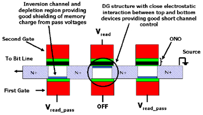
Cross-sectional schematic of the proposed dual-gate thin-film-transistor semiconductor-oxide-nitride-oxide-semiconductor (DG-TFT-SONOS) type Flash structure (source: Schiltron Corp.)
Unique properties of antimony in silicon allow multilayer monolithic 3-D stacking. The “Schiltron Solution” uses a double-gate (DG) which provides close electrostatic interactions to control short channel effects. The DG structure is certainly scalable (see figure), reportedly has zero pass disturbs, and is easily stackable due to “freezing” of the source/drain dopants. With 48nm Lg and 35nm channel thickness in the burried gate, a loose definition could term this a “nanowire” device, which would suddenly make chips based on this structure the nanowire memories that are the closest to production reality.
To erase the cell, you invert the back gate and apply the erase voltage to the top gate. Since only electrons, not hot holes, are needed to erase this device it lends itself to cycling endurance. You can use the thin tunnel oxide without damage; 32 cell strings tested under accelerated lifetime conditions showed that the devices should withstand 10 years at 85°C with good results.
Only industry standard CMOS processes and materials are used to fab this device, allowing Schiltron the flexibility of developing the integrated process flow with any advanced digital CMOS foundry. “We’re riding on the coat-tails of CMOS and the standard tooling,” explained Schiltron founder and president Andrew Walker. More details in this week’s BetaSights Newsletter. –E.K.
