Monday, March 16th, 2009
The BetaBlog of March 5th was originally titled “Amkor chooses TMV not TSV for PoP” and Amkor’s stalwart vice president of business development Lee Smith contacted BetaSights to correct the impression that Amkor may have chosen to not work on TSV. I’d intended the original title to be somewhat playful; since TSV is chip-level while TMV and PoP are of course inherently package-level technologies, the title called into question when TSV might be used in place of PoP. The title has been changed to “Amkor’s TMV PoP will go to 0.3mm.”
The graphic shown in the March 5th post was a schematic of a TMV PoP using wire-bonded chips. However, the TMV package can just as easily handle chips with TSV. “If you needed high density, you could combine TSV and TMV to achieve very hgh density stacking,” explained Smith. “It’s not a straight approach to choosing one or the other.” What about functional overlap between TMV and so-called “2nd-generation” TSV with ~100 embedded conductors? Smith insists that the technologies are completely complementary.
Amkor’s motivation with TMV is to provide a low-risk path to extend PoP for it’s customers. “They want to maintain the current SMT infrastrucure, so a new bottom package technology was needed,” explained Smith. In the next 12-14 months, low-power DDR2 is being specified for stacking on top of mobile processors, and the bottom package to memory package interface for some will drop from 0.65mm to 0.5mm or 0.4mm pitch according to Smith.
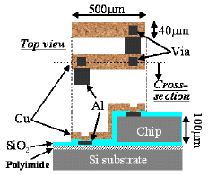
Besides PoP and TSV, the other known 3D stacking solution is edge-contacts (see figure, shown by Tohoku University in Session 20.5 of IEDM 2008). While certainly providing unique capability, the cost/performance of edge-connnections has always limited such approaches to niches like Mil/Aero. Thus, while edge-connection technology exists, it must win competiton with wire-bond, flip-chip, and now TSV, and that may be difficult. –E.K.

