Thursday, March 26th, 2009
German and French teams are combining EUR 14.5m investment into development of strained-silicon on insulator (sSOI) technology under the DEvice and CIrcuit performance boosted through SIlicon material Fabrication (DECISIF) program. The work will combine original research results from Research Center Juelich and Leti/Soitec to try to lower costs and defect-densities in the creation of 300mm sSOI wafers for microprocessors and consumer systems-on-chips. Work will start on 45nm node structures, with extension to 22nm planned.
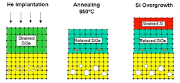
The Federal Ministry of Education and Science (BMBF) granted EUR 8.1m for DECISIF Another EUR 6.4m will be contributed by the project partners GlobalFoundries Dresden, Siltronic, Aixtron, Research Center Juelich, and the Max Planck Institute of Microstructure Physics. French partners STMicroelectronics, Soitec, and Leti will also collaborate within the scope of the EU-project Medea. Prof. Siegfried Mantl of Research Center Juelich, the project coordinator for Germany, told BetaSights that they will investigate strain/stress on the wafer level (see figure showing the “Juelich process”) as well as on the transistor level with new stressor methods.
The Juelich process starts by growing a cubic-Si/strained SiGe/Si heterostructure. Then, the pseudomorphic SiGe layer is relaxed using a He+ implantation and an annealing step. The relaxation of the SiGe layer establishes the elastic strain in the top Si layer. The strain generated depends on the layer thickness and the degree of relaxation of the SiGe layer. For top Si thicknesses up to 8 nm (over 150 nm thick Si0.74Ge0.26), 100% strain transfer is observed.
These global strain techniques will be combined with new techniques to create locally strained silicon to reach an exceptionally high mobility of the charge carrier within transistors. The objectives of this project are to integrate performance boosters in fully- and partially-depleted SOI for Low Power and High Performance, to validate these technologies by fabricating complex 45nm node demonstrators directly comparable with bulk Si and to develop design kits and SOI-adapted circuit design for evaluation by application designers. More on sSOI and exclusive comments from Mantl will be in the next BetaSights Newsletter. –E.K.
Tags: 22nm, 32nm, 45nm, CVD, EDA, epi, IC, implant, integration, Material, Si, SiGe, SOI, sSOI, strain, wafer

