Tuesday, March 31st, 2009
Semilab, founded in 1990 and headquartered in Budapest, Hungary, is spending cash to continue to expand its portfolio of fab metrology offerings. Today, the company announced it has acquired Advanced Metrology Systems (AMS) and QC Solutions. The two Massachusetts-based metrology companies expand Semilab’s family of scalable, flexible solutions to help semiconductor and solar manufacturers characterize materials. Semilab claims an installed base of over 3000 metrology systems worldwide.
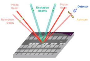
AMS offers solutions for fast and detailed characterization of 3D etched structures including contacts and trenches using model-based IR (MBIR) technology; metal film thickness on product wafers using acoustic surface wave profiling (see figure); and high speed online mapping of low-k material properties. AMS’ award-winning products are installed in the fabs of IBM and AMD. AMS will now become part of a Massachusetts division of Semilab known as Semilab AMS. QC Solutions offers patented, non-contact, non-destructive systems for the fast and repeatable measurement of the electrical properties of epitaxial and implanted silicon wafers. QC Solutions will also become part of Semilab AMS.
“With these acquisitions, we are expanding our ability to provide a full set of metrology solutions to support basic material characterization in everything from R&D settings to fully automated production lines,” said Dr. Tibor Pavelka, one of the founders, now president and CEO of Semilab. “We believe investing in the semiconductor market, even in these tough times, will enable us to continue our nearly 20 years of growth and profitability and meet the metrology needs of the market presented by the drive to smaller nodes and new materials.”
Both acquisitions were all cash transactions. QC Solutions and AMS are the latest metrology companies to be acquired by Semilab. In 2008, the company purchased the assets of French metrology equipment specialist Sopra. In 2008 Semilab acquired the majority of SSM of Pittsburgh, PA, and the Boxer Cross metrology IP from Applied Materials. Semilab also started a JDP with IMEC for high-k dielectric metrology last year. More about specialty metrology in the next issue of the BetaSights Newsletter. –E.K.
Tags: 45nm, epi, fab, high-k, IC, implant, Material, metal, metrology, PV, solar, test, thin-film

