Friday, April 10th, 2009
The Materials Research Society (MRS) Bulletin for April 2009 covers some of the newest engineering work for the growth of large and pure electronic crystals. In this week before the annual MRS Spring Meeting in San Francisco, this issue of the monthly MRS members magazine provides an excellent overview of the latest technologies used to grow Si, Ge, GaAs, InP, as well as perovskite and other semiconductor crystals on industrial scales. The BetaBlog next week will be reporting from the San Francisco event.

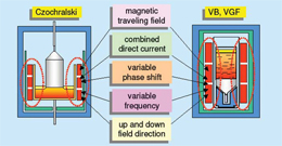
Traveling magnetic fields in Czochralski (left) and vertical Bridgman or vertical gradient freeze (right) crystal growth tools generated by heater-magnet modules (source: MRS Bulletin)
Industrial bulk crystal growth from the melt has gradually evolved in complexity to be able to ensure ever reduced costs and defect counts, typically through increases in size of the melt and crystal. However, larger melts display convective perturbations and even turbulences that produce large temperature fluctuations that induce growth rate oscillations seen as “striations” within the grown crystal. Melt convection non-uniformity may distort the melt-solid interface leading to higher dislocation density. Today’s state-of-the-craft for 300mm diameter Si growth uses traveling magnetic fields from heater-magnet modules (see figure) in both Czochralski (left) and vertical gradient freeze (VGF) (right) crystal growers.
Scheel and Schulz-DuBois (J. Cryst. Growth 8/304, 1971) introduced the accelerated crucible rotation technique (ACRT) for high-temperature solution growth. The technique has been used to grow a wide variety of crystals. In zone melting techniques from melt solutions, the ACRT enhanced the zone mixing and, therefore, the growth rate stepped up by approximately one order of magnitude. Recently, ACRT was used for the unidirectional solidification of photovoltaic (PV) multicrystalline silicon with improved carbon homogeneity and reduced impurity precipitates (Bairava Ganesh, et al., Cryst. Growth Des. 8/2525, 2008). ACRT transfers momentum from the crucible wall into the melt by modifying the rotation rate of the crucible as a function of time; the container accelerates from rest up to a maximum rotation rate followed by a deceleration or even a change in direction.
Among other articles, the issue also details recent progress in the growth of AlN and GaN crystals. The general problem of manufacturing low defect wafers of desired size is still an open issue. Physical vapor transfer (PVT) seems to be the best known method for AlN crystal growth, delivering dislocation densities as low as 1000/cm2 (100x improved from commercially available crystals today), but still requires a lot of tedious engineering work to increase the yield and scale the process beyond 25mm diameter crystals. Hydride vapor-phase epitaxy (HVPE) today provides modest quality GaN crystals, while improvements in quality and size up to 100mm diameter may be possible with the ammonothermal route under development by Ammono in Poland. More on crystal growing in the next BetaSights Newsletter. –E.K.
Tags: crystal, defect, epitaxy, GaAs, Ge, growth, IC, InP, PV, Si, wafer
