Tuesday, April 14th, 2009
sp3 Diamond Technologies – the supplier of diamond film products, equipment, and services – today announced it is taking orders for 50mm and 100mm silicon on diamond (SOD) wafers for use as Gallium Nitride (GaN) substrates. Having worked with Nitronix on the GaN, sp3 Diamond Technologies uses combinations of thin-film depositions, wafer thinning, and layer transfer techniques to create SOD wafers that improve thermal conductivity compared to Si or SiC substrates. Work now is for the development of 150mm wafers for use as laterally diffused metal oxide semiconductor (LDMOS) substrates.
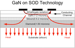
 100 mm SOD substrates were fabricated using hot filament diamond deposition on high resistivity float zone silicon wafers, followed by flipping and grinding the original substrate to create a thin silicon seed layer for the GaN epi layer. MOCVD technology was then used to grow the buffer, GaN and AlGaN device layers (see figure). Two different GaN layers were grown to investigate the effect on device performance as well as structural characteristics of the wafer. GaN devices layers were shown to be of sufficient quality to make HEMT transistors.
sp3’s SOD wafers deliver a high performance path for devices designed for WiMax base stations and other commercial and military broadband and high power switching applications. “High-power, high-frequency devices – such as high power radar and RF amplifiers, and DC to DC and AC to DC converters – have performance limitations due to the physical structure of standard silicon substrates,” said Dwain Aidala, president and COO of sp3 Diamond Technologies. “sp3’s SOD wafers deliver industry-leading performance, are scalable up to 300 mm and are available at a lower cost than alternative diamond-based solutions or traditional SiC substrates.”
The diamond heat spreading layer directly under the junction can allow for more than a 100% increase in power levels compared to silicon substrates alone, and a 50-80% increase when compared to SiC, at a fixed junction temperature. At fixed power, they can reduce junction temperature by more than 50 degrees compared to GaN on silicon or SiC. GaN growth on SOD reportedly yields epi films equivalent to GaN on silicon. –E.K.
Tags: 100mm, epi, GaN, HEMT, IC, LDMOS, materials, MOCVD, Si, SiC, SOD, thin-film, wafer
