Friday, May 1st, 2009
Leaving California for the first time, the 12th annual IEEE International Interconnect Technology Conference (IITC) will take place in Sapporo, Japan, June 1-3. With lithographic shrinks in 2D dimensions slowing, interconnects between chips in packages and in 3D stacks will be the driver for increased density and functionality in ICs. Thus, the more than 80 technical presentations at IITC this year will show the way toward the most likely major innovations to come in the IC fab ecosystem.

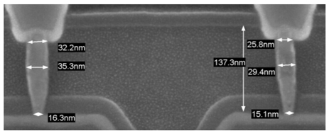
SEM cross section of 15-16 nm Cu contacts post-anneal. There is no Cu diffusion through the Ru to the silicide, and no void formation. (source: IBM)
The semiconductor industry has 65nm and 45nm node chips in volume production, most using dense, non-porous, low-k dielectrics made from SiCO(H) films (k~2.7-3.0) to isolate Cu lines, Cu vias and W contact plugs. As the world’s leading IC foundry, TSMC will present an invited paper on, “Challenges of Low Effective-K Approaches for Future Cu Interconnect.” At the smallest dimensions the relatively higher resistance of W limits performance, so Cu contacts are needed. IBM Alliance researchers used Cu contact metallization with a CVD ruthenium (Ru) liner to demonstrate the world’s smallest fully-functional 22nm node 6T-SRAM. They will show the extendibility of Cu contact metallization to 15nm contacts (see figure).
The conference will continue its 12 year history of addressing issues of interest to both the development and and manufacturing communities:
- Materials and Unit Processes
- Process Integration for Logic and Memory
- Process Control / Modeling
- Reliability
- TSV and 3-D Interconnects
- Interconnect Systems
- Packaging
- Novel Materials and Concepts.
The plenary keynote presentation will be by Satoru Fujikawa, Director, R&D Strategic Semiconductor Development Center, Panasonic on “Integrated Digital AV Platform ‘UniPhier’” which is the company’s 45nm node SoC. An invited paper on chip-package integration, “Interconnection with Copper Pillar Bumps: Process and Applications,” will be presented by Choon Heung Lee, Amkor Korea Technology. Hiroshi Toyoda, the 2009 IITC Publicity chair commented, “We will be able to incorporate a wider range of participation from Asia this year. These new perspectives will benefit all participants.”
New package architectures that use fan-out and through-mold-via (TMV) interconnects, combine with flip-chip and wafer-level packaging (WLP) to create dense IC systems with unique thermal management issues. NEC and Tokyo Institute of Technology researchers will present a paper on 3D packaging technology called SMArt chip connection with Feed Through Interposer (SMAFTI). The team implemented a new die bonding process and multilayer interconnect technology to form over a thousand parallel interconnects between memory and logic dies. They characterized the interlaminar horizontal wiring by S-parameter measurement up to 40 GHz and confirmed its potential for high-speed signal transmission at over 10 Gb/s.
“The needs of the industry have demanded IITC to adapt, both in the scope and content our technical program,” said J. D. Luttmer of DRS Infrared Technologies and IITC 2009 General Conference Co-Chair. “By rotating our forum to Asia and Europe in 2011, IITC is exposing the interconnect community to a wider audience in each region. Additionally, by focusing on emerging technologies like 3D integration, we can provide our constituents with up-to-date information to guide them as they make both strategic and tactical decisions.”
In 2010, the conference will return to the U.S., to be held at Burlingame, CA. This year, some 600 scientists, engineers, exhibitors and other interconnect professionals are expected to gather in beautiful Sapporo. The conference will be preceded by a one-day Short Course on Sunday, May 31, and also will feature a product exhibition. Lunch will be provided for registered attendees each weekday, and the popular supplier seminars will be held Monday and Tuesday nights. –E.K.
Tags: 22nm, 32nm, 3D, 45nm, 65nm, contact, Cu, dielectric, IC, integration, low-k, TSV, W
