Tuesday, July 7th, 2009
Applied Materials has extended physical vapor deposition (PVD) technology to be able to coat the sidewalls of 22nm node structures. “It’s been validated, it’s been shipped, and it’s been qualified in pilot lines for both logic and memory,” asserted Marek Radko, Applied Materials’ BEOL GPM Manager, in an exclusive interview with BetaSights. Separately, the company has also launched a lower cost PVD tool targeting chip packaging lines. Based on multiple successful beta site tests for each tool, these offerings significantly broaden the company’s deposition product lines.
With >8 layers of on-chip interconnects typical for advanced ICs today, the majority of thin-film deposition tools are tied to dual-damascene copper process flows. So while the dielectrics are deposited as blanket layers, the metals must be deposited into ever smaller spaces as feature sizes continue to shrink. Electro-chemical deposition (ECD) grows the copper lines from barrier and seed layers deposited by PVD.
PVD (with variations known as “sputtering” and “evaporation”) has been used to coat metals on ICs for decades. The metal source may be a solid “target” or a liquid melt, but in either case energy is applied to vaporize the metal inside of a vacuum chamber, and metal atoms fly off to coat the surface of substrates. One of the major limitations of PVD is that the coating is “line of sight” from the source to the substrate, such that the sidewalls of features on non-planar substrates are difficult to cover. The smaller the structure, the more difficult it is for PVD to coat sidewalls.
 Chemical-vapor depostion (CVD) and atomic layer depostion (ALD) technologies use chemical precursors (instead of the pure material used in PVD) that are tuned to react only on the substrate surface, so growth on sidewalls may be nearly equal to that on the top of structures. Thus, as the IC fab industry continues to shrink circuit features, CVD and ALD have been considered as the logical replacements for PVD. However, the cost-of-ownership (CoO) for these other technologies is almost always higher compared to PVD, and the chemical reactions involved may leave trace quantities of undesirable reaction byproducts in the final film. For these and other reasons, extending PVD to be able to coat smaller structures has been pursued for many years. “We’re still working on PVD extendibility,” said Gary Miner, Applied Materials’ Front End Products Group chief technology officer, in an exclusive interview with BetaSights. “At some point there will be a transistion, but it’s very hard to predict when it will switch. Through 22nm it’s still going to be PVD.”
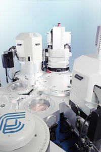
The new “RFX” extensions to an “Endura” chamber include new controls: uniform magnet motion (UMM) behind the target, and two different RF frequencies coupled into the chamber at different points. Flux in traditional magnetron PVD has non-optimal directionality due to non-uniform target erosion which results in within-wafer variation in sidewall coverage. A new spiraling path for the magnet (driven by interlocking gears like in the old “spirograph” child’s toy) provides far more uniform target use.
A 2 MHz RF coil above the wafer induces a secondary plasma to direct ions and improve the coverage in the bottoms of nano structures. Resputtering to optimize copper sidewall coverage is controlled by 13.56 MHz RF coupled through the electro-static chuck (ESC). You can tune the resputter to optimize different recipes for structures such as dual-damascene interconnects, trenches, or through-silicon vias (TSV).
Applied Materials claims that ~10% of the company’s total PVD sales has been for Cu barrier/seed applications, represented by 490 systems delivered to fabs. The company expects to gain sales from the major shift to Cu for memory expected over the next 6 quarters. Current generation PVD tool owners can upgrade chambers in the field to include “RFX” sub-systems.
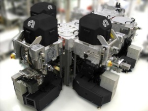
 In contrast to the extremes of process control and cost needed for the smallest commercially manufactured device structures on the planet, the company’s new “Charger” tool is designed for the modest control needed at super-micron dimensions. Target applications include under bump metallization (UBM), redistribution layers, and CMOS image sensor (CIS) lines, where there is always extreme price sensitivity. The tool targets >85% avalability and throughput >30 wph, with 5000 wafers MTBPM (mean time between preventative maintenance). Multiple systems have been shipped and are in production.
The increase in MBTPM is mainly due to the company’s new “Isani” preclean chamber, using a thin plasma sheath to provide the force for an argon plasma to sputter polyimides and nitrides from the wafer surface. The sputtered material adheres to specially designed shields, where surface textures and thermal coefficients of expansion (TCE) have been tuned to allow for the thickest possible buildup before the chamber needs a PM. –E.K.
Tags: 22nm, 32nm, barrier, barrier/seed, Cu, damascene, fab, IC, metal, PVD, seed, TSV, UBM
