Wednesday, July 22nd, 2009
At SEMICON West and Intersolar North America last week in San Francisco, crossing guards danced to keep the throngs away from the vehicles at the corner of 4th and Howard, as many people flowed back and forth between the shows co-located across 4th Street from each other. SEMICON West, down ~30% in size from last year, still fill most of both North and South Halls in the Moscone Center. Intersolar, continues to grow and now fills most of all three levels of West Hall. Excellent technical presentation and keynote addresses, leading exhibitor booths, standards meetings, and many side events combined to make this an intense work week.
SEMICON now includes focused technical presentation sessions called “TechXpots,” and this editor moderated the first session on device scaling entited, “Advanced Processes and Materials for New Devices.” Raj Jammy, SEMATECH VP of Materials and Emerging Technologies, provided an extremely authoritative overview of the scaling challenges and currently known solutions to get to 16-22nm node devices. He showed that new materials (like III-V and II-VI compounds) and new devices (like finFETs and quantum well devices) allow for evolutionary extensions of CMOS, and when eventually needed we may be able to lead a revolution using graphene transistors and nano-electromechanical system (NEMS) switches.
Much of the near-term CMOS processing challenge involves non-equilibrious rapid thermal processing (RTP) to be able to control atomic layers in manufacturing, as described by Paul Timmons of SEMATECH OEM partner Mattson Technologies. Many of the slides shown in TechXpots and keynotes can now be found online, and all are worth reviewing.
Humans focus on large negatives while ignoring small positives, and so we notice and remember when a big company disappears from a market, but never notice the many upstarts that grow to serve that same market. A bogus “common sense” tends to develop when people fail to check the data, and eventually myths arise in a market. In the IC fab market, it is common for people to feel and express that maturation has led to inevitable consolidation, and that new fab technologies adoption is slowing down.
These two myths were ably dispelled by Mentor Graphics Corp. Chairman Wally Rhines in his Wednesday morning keynote; download the full slide set from SEMI. Drawing on data from leading analyst houses, Rhines showed that the market share held by the top 10 IC suppliers and even the top 5 DRAM suppliers has remained nearly constant over the decades. His company’s own data on the rate of adoption of new technology nodes—as seen in design starts—seems to confirm reticle and wafer start data showing that new nodes are being used about as fast as in the past. Examples of 45nm and 32nm node IC technology opening up new end-uses to drive more IC unit volumes include CMOS image sensors, cell phone handset SoCs, and embedded software applications allowing chips to be ever more functional. Rhines observed that—unlike in past downturns—there was no fab equipment boom in recent years, so there is not supposed to be very much excess IC fab capacity in the world today.

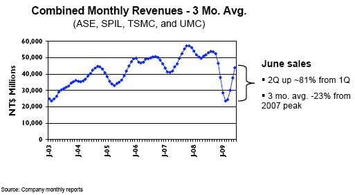
The official data shown during the SEMICON press conference indicate that the IC fab industry has already bounced off the bottom of this cycle (see figure). This last downturn has seen many segments of the IC fab ecosystem revenues down to 2001 levels, while the last quarter has typically seen improvements up to 2005 levels. SIA/WSTS data for May 2009 show that IC unit shipments declined by 36.7% 4Q08-1Q09, which was the largest percent decline and the steepest slope of any downturn in history. SEMI’s silicon wafer area shipment data—not including PV wafers—show that fabs had rapidly cut their wafer starts over the last year. Thus, it seems that there really should be minimal IC inventory in the world, and the second half of this year should see a slow and steady increase in production.
The PV fab industry is still very immature. Investors still see it as an intellectual property (IP) land grab, and like all information flows to be one-way in. Technologists seem like teenagers; first to think of everything, and haven’t yet learned how to share well. Consequently, essentially all process information is consider novel and proprietary, so it was refreshing that some of the InterSolar North America presentations discussed fab technologies. Evergreen’s ribbon silicon pulling technology is genuinely unique and currently in mass production; yet it seems rather immature with a lot of room for improvement in both fundamental material properties as well as fab costs. Konarka Technologies has retrofitted an old Polariod factory in Massachusetts to be able to produce 1 GW of organic PV panels each year.
The immaturity of the PV industry can also be seen by wide demand swings. With demand for PV still limited by global financial insanity, and with the “overhang” inventory of some GW of modules allegedly stuck somewhere in Spain, the demand for PV fabs is anything but certain today. However, with PV currently supplying somewhere near 0.02% of global energy use—glibly characterized as a “rounding error” by one presenter—there’s nearly endless growth potential.
More details about SEMICON, InterSolar, and growth in PV, MEMS, and non-silicon semiconductor fabs will follow in future BetaBlogs. –E.K.
Tags: 22nm, 32nm, IC, Material, OEM, PV, SEMI, Semiconductor
