Friday, September 18th, 2009
At SEMICON West this year, ASML announced tools that fleshed out their Holistic Lithography scheme introduced at SPIE’s Advanced Lithography Symposium in February of this year. The key idea of Holistic Lithography, according to Bert Koek, senior vice president of the applications products group at ASML, is integrating computational lithography, wafer printing, and process control to enable shrink towards 32nm using 193nm water immersion exposure tools. The computational facet reduces the process window shrinkage, advanced tooling enables volume manufacturing, and new metrology methods insure that the tools remain centered on the process window.

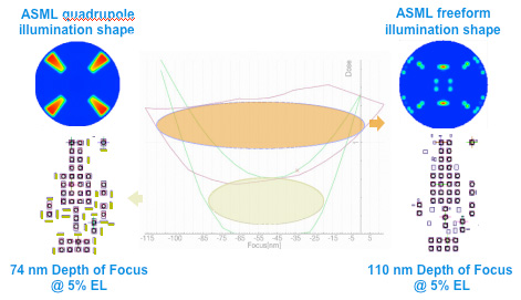
The same contact hole pattern (lower right) can be printed with improved process window (center) using FlexRay illumination (upper right) than with quadrupole illumination and a mask with sub-resolution scatter-bars (green). (source: ASML)
The Tachyon Source-Mask Optimization announced in February addressed design issues by incorporating a software model of the exposure tool in the OPC/illumination optimization process. Specific tool tuning knobs could be set to optimize the process window for key design clips. The illumination geometry, however, was constrained to what could be implemented with diffractive optical elements, which had to be ordered, fabricated, and delivered along with the mask. The FlexRay illumination system, announced at West, replaces the diffractive element with a micro-mirror array of 4000 elements (see figure), each of which could be set independently in near real time. That allows more complex illumination schemes which can be matched to the actual tool and delivered reticle. According to Koek, free-form illumination enables larger process windows with simpler OPC schemes (see figure), reducing mask costs. “The idea is to push the complexity from the mask to the illumination source, which is purchased only once,” said Koek. Free-form source tuning can also correct wafer CD biases due to mask fabrication realities, while maintaining OPC validity, claimed Koek.
Once the best process window is achieved, the challenge becomes preventing the exposure tool from drifting away from optimum conditions. The new ASML BaseLiner scanner control system insures optimum critical dimension uniformity (CDU) and overlay without maintenance actions that interrupt production. Instead, single monitor wafers are exposed once or twice a day and analyzed using ASML’s not-so-secret YieldStar scatterometry system, which determines corrections that can be implemented using control “knobs” on the scanner. By measuring 4000 targets on the monitor wafer offline, YieldStar (supplied as part of the BaseLiner scanner stability package) simultaneously calibrates focus, dose, and overlay. Koek showed data in which this system resulted in a 3X improvement in ASML’s 1900i tool overlay to <5nm over 1 month.
ASML offers its various Holistic Lithography products and services as Eclipse packages, optimized for node, layer and process. Not all manufacturers will want to use the new ASML products for all the functions, so Eclipse assembles those needed as blocks with the option to interface with existing tools and processes. As the industry approaches the limit of water immersion lithography, intelligent integration of wafer lithography, computational lithography and process control will become crucial. The ASML Eclipse system with its hardware and computational features integrated holistically into production, potentially offers one way to continue shrinking devices with acceptable yield. –M.D.L.
