Wednesday, August 12th, 2009
At the SEMICON West 2009 Device Scaling TechXPOT, moderated by this editor, SEMATECH’s Ray Jammy reviewed the latest results in scaling CMOS transistors. “We are litererally running out of atoms,” explained Jammy. “You can see the number of atoms in a gate dielectric.” When you have such thin layers, how do you control device parameters? Metrology is also an issue; how do you see what you have made?
MOSFET scaling requires the control of the ultra-small and control. New materials are generally the solution, with more complex combinations of elements capable of providing high mobility with low leakage. Multiple gates (either dual-gate planar, or multi-gate fin) and nanowires may provide better electrostatic control.
Jammy also discussed extensions of high-k (HK, where “high” is conventionally used to denote the modest k range of 10-20) interface engineering work needed to ensure ultra-shallow junctions for source and drain device regions. Derived from the “dipole engineering” of aluminum oxide (AlOx) for NFET and lanthanum oxide (LaOx) for PFET devices so that both can use a single metal contact, SEMATECH has been working on ways to use a “simple nitrogen-based interface” to lower the S/D contact resistance by an order of magnatude. The contact resistance is dominated by NiSix.
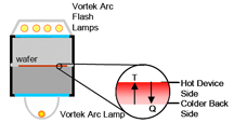
 SEMATECH partner Mattson Technologies provides the rapid thermal processing (RTP) tooling used in the work (see figure) on gate and junction formation. Millisecond annealing is achieved by ramping the whole wafer up to a moderate temperature, and then flashing a light source for such a brief period that only the top side of the wafer is heated to a higher temperature. With proper control, this results in the bulk of the wafer being a heat sink to help rapidly cool the top side. Mattson’s RTP technology director, Paul Timans explained that different RTP approaches require different ion implant recipes to ensure optimum results. For example, changing to a millisecond anneal from a Spike anneal resulted in non-ideal Halo implant activation, such that dose and energy had to be adjusted to ensure proper device results.
For sub-30nm-node devices, preliminary data show that leakage from the gate dielectric alone is starting to dominate the power, so gate leakage must be controlled regardless of gate equivalent oxide thickness (EOT) or S/D structures.
High-k dielectrics based on hafnium oxides that may be alloyed with Si and N are the current standard for CMOS gates <45nm node. Whether integrated in “gate-first” or “gate-last” flows, the HK layer currently sits on top of a ~1nm thick SiON interface layer (IL). The IL generally grows from the channel surface during the HK gate deposition process, such that it has conventionally been considered as an inevitable part of the structure.
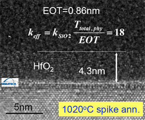
 A later Device Scaling TechXPOT presentation by SEMATECH director of front-end processing Paul Kirsch on HK and metal gate (MG) for 22nm node and beyond devices showed breakthrough results on ability to reduce the IL to nothing. Zero interface layer (ZIL) HK uses HfOx directly on Si capped by MG (see figure). The TEM image shows ~10° angular misalignment between the crystalline HfO2 and the underlying Si. Somehow, the process flow ensures both ZIL and almost no interface defects.
In a private message to BetaSights, Kirsch mentioned that, “We worked pretty hard to control the Hf : O ratio during the dielectric deposition. With the ‘correct’ Hf : O ratio, we were able to keep the annealing for S/D the same (i.e. a 1020C spike). This is useful for both gate first and gate last approaches.”
SEMATECH labs are already working on HKMG over both Ge and InGasAs with ZIL. Metrology for HK is VUV reflectometry (Ref: Metrosol), where one tool provides LaOx, AlOx, HfOx, HfSiO, SiOx interface measurements.
Monolayer caps of molecules to control work function have recently been explored by researchers at Rice University and North Carolina State University (NCSU). James M. Tour (Rice) and Paul D. Franzon (NCSU) et al. published “Controllable Molecular Modulation of Conductivity in Silicon-Based Devices” (Ref: J. Am. Chem. Soc., 2009, 131 (29), pp 10023–10030), showing that a molecular monolayer, covalently grafted atop a silicon chanel, can play a role similar to gating and impurity doping.
Charge transfer occurs between the silicon and the molecules upon grafting, which can influence the surface band bending, and makes the molecules act as donors or acceptors. The partly charged end-groups of the grafted moleculular layer may act as a top gate. The doping- and gating-like effects together lead to the observed controllable modulation of conductivity in pseudometal oxide semiconductor field-effect transistors (pseudo-MOSFET). If such grafted molecules can withstand 450°C to allow for standard metal interconnect processing, then such devices could be easily mass produced in current IC fabs.
If you are interested in HKMG technology, then you definitely want to be in San Francisco during August 24-26 for the IEEE-SEMATECH 6th International Symposium on Advanced Gate Stack Technology. Top researchers from GlobalFoundries, IBM, Intel, Samsung, TI, Qualcomm, and major universities will present their findings on unit processes, integrated flows, and future devices. –E.K.
Tags: 22nm, 32nm, 45nm, ALD, dipole, fab, gate, HfO2, high-k, HKMG, IC, junction, R&D, RTP
