Friday, August 21st, 2009
James Quinn, CEO of Replisaurus, has been very busy executing for the last few years to bring his vision of a new metallization technology to the IC fab industry. Targeting the formation of Cu interconnects for advanced packaging applications, Quinn has assembled a great team to work with CEA-Leti and other industrial partners on a selective electro-chemical deposition (sECD) technology called electro-chemical pattern replication (ECPR).
Also known as patterned ECD, sECD has been explored for many years, with a recent failure in the form of the NuTool technology acquired and abandoned by ASM. Among the issues with prior attempts to develop a manufacturable sECD technology, electrical current non-uniformity across the wafer was inherent due to horizontal flux across templates. In contrast, Replisaurus uses a thick bus to shuttle current across the template, with dielectric isolation from the Cu pattern such that the current flux during ECD is essentially purely vertical.
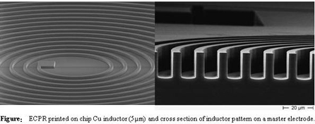
 The Replisaurus technology uses 15µm deep trenches filled with 10µm of Cu, and transfers only ~5µm per wafer pass (see figure), typically within one minute. The typical resolution is 5µm/5µm (line/space), though 500nm/300nm has been demonstrated. A reusable master electrode is used as a template to fabricate work-master patterns. The work-master provides pattern definition and metal deposition in one step, thus eliminating the need for traditional photolithography and plating. A single tool can thus replaces 6 tools in a typical though mask plating process (coat, expose, develop, descum, electroplate, and strip), reducing capital investment from 10-30M down to only 4-8M euros.
The template mastering has been established through a joint venture (JV) with Leti called Replisaurus Mastering, and the program is already up and running at Leti’s facility in Grenoble. “The mastering process is a central part of our business model and a unique component of our technology, so Leti’s practical, business-oriented approach to IP rights was a major factor in our decision to partner with them,” said James Quinn, CEO of Replisaurus. “We are moving forward according to plans to roll out our technology, and through this partnership Leti will support us in transferring it to a foundry partner.”
Since Leti has 8,000 m2 of state-of-the-art 200 mm and 300 mm wafer clean rooms, and 1,200 employees running in “24/7 mode,” the organization can easily supply the templates. Alan Cuthbertson, coming from senior management positions in Cu and low-k interconnect technology development for 130nm and 90nm node ICs, is Replisaurus’ vice president of Mastering Technology. “CEA-Leti has advanced capabilities with CMOS and MEMS applications that will be a great testbed for our technology as we look to apply it in other application areas,” said Cuthbertson. “We will focus on 200mm silicon and 300mm through this project and Leti’s world-class facility is the perfect place to enhance our technology for the chip market.”
Replisaurus also has established a “common laboratory agreement” with Leti. Under the multi-year agreement, Replisaurus and Leti personnel will collaborate on optimizing the development of reusable master electrodes. The two sides will also investigate the opportunities for this technology in new applications, notably in key growth sectors such as integrated passives, copper pillars, and 3D integration. The team will optimize electrode design and fabrication flow for each application area, ensuring the best yield, endurance, and cycle time.
“This new project with Replisaurus is a very exciting challenge as we help integrate its innovative clean metallization technology into a high-volume manufacturing solution. All of the necessary technical developments are already underway, and this collaboration got off to a great start,” said Laurent Malier, general manager of CEA-Leti. “In addition, access to ECPR technology through this agreement will enable Leti to position itself at the leading edge of research into advanced interconnect and device packaging technologies for diverse applications.”
Mike Thompson joined Replisaurus as COO last fall, after 17 years at STMicroelectronics Crolles, France, most recently as the deputy CTO of STMicroelectronics, with responsibility for CMOS R&D, covering design and process technology and the Crolles 200-mm and 300-mm operations. Prior to this, Thompson also helped establish ST’s participation to the IBM bulk CMOS Alliance and the Crolles2 Derivatives Technology Alliance in Crolles. –E.K.
Tags: Cu, deposition, ECD, IC, interconnect, Leti, MEMS, metal, packaging
