Wednesday, August 26th, 2009
IMEC/F-IZM/SUSS/TM vs. SEMATECH/Leti/EVG/Brewer.
The leading R&D consortia have aligned (pun intended) with leading equipment and materials suppliers to create ultra-thin silicon wafer handling technologies for 3D ICs. With the ability to shrink circuit dimensions in 2D becoming ever more difficult, most of the world’s IC fab leaders are evaluating the use of the 3rd dimension. In addition to the EMC3D suppliers’ consortium, all of the leading IC technology R&D consortia (IMEC, Fraunhofer-IZM, Leti, and SEMATECH) now have 3DIC programs in place with equipment and materials suppliers.
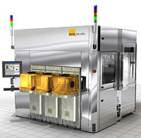
 IMEC and SUSSMicroTec recently started a joint development program. Together, they will develop permanent bonding, temporary bonding and debonding processes for 3D system integration, including through-silicon-via (TSV) manufacturing. IMEC will use SUSS ’s XBC300 production wafer bonder platform (see figure) to develop 200 and 300mm permanent metallic interconnect bonding, as well as temporary bonding and debonding solutions for its 3D-stacked Interconnect and 3D Wafer Level Packaging technology. The bond cluster also includes a spin coater, a low force bonder and a plasma chamber. The XBC300 temporary bond configurations are available for development and high volume needs.
For its 3D IC technology, IMEC uses a process flow where TSVs are realized in a single-damascene process that is performed immediately after active-device and contact processing but prior to formation of interconnect metallization layers. This process enables small via diameters of 1–5micron. After completion of the back-end wiring, silicon is removed from the bottom of the substrate to open the buried TSVs. Dice or wafers subsequently are stacked and interconnected in a wafer bonding step.
“We are very pleased to co-develop with SUSS MicroTec the processes for permanent and temporary wafer bonding for our 3D technologies,” said Eric Beyne, Program Director of IMEC’s Advanced Packaging and Interconnect Research Centre. “In particular, the debonding and handling of very thin wafers ranging from 25 to 50 µm is an especially challenging and critical process. We are convinced that the versatility of the SUSS wafer bonding and debonding tool platform will contribute to bringing 3D integration technology to maturity.”
SUSS’s XBC300 production wafer bonder is matched with material from Thin Materials (company in stealth mode) to create the temporary bonding solution to be used for challenging thin wafer handling. This material is capable of handling wafer processing temperatures in excess of 250°C, but can be de-bonded at room temperature. Fraunhofer-IZM works with the team at Thin Materials, too.
“Thin Materials’ technology for temporary bonding perfectly complements our process offering portfolio for 3D Integration and Packaging”, confirms Frank Averdung, President and CEO of SUSS . “Partnering with Thin Materials allows us to offer our customers a wide variety of temporary bonding technologies according to their specific needs.” Together with its partners 3M, Disco, DuPont, NEXX Systems, Surface Technology Systems, and Thin Materials, the company hosted a TSV 3D Integration workshop introducing solutions for temporary bonding and thin wafer handling on July 15th during SEMICON West.
Meanwhile, CEA-Leti continues to work with EVG and Brewer Science on temporary bonding for 3D ICs. Thorsten Matthias, director of technology for EVG North America, presented “Thin Wafer Handling and Chip Stacking for 3D Integration” at the SEMICON West Test, Assembly & Packaging TechXPOT.
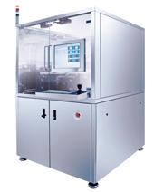
 SEMATECH has purchased an EV Group wafer bonder with “SmartViewNT” technology (see figure) for TSV wafer-to-wafer (W2W) bond alignment. The alignment uses a high-precision stage that comprises top- and bottom-side microscopes to ensure the highest degree of accuracy for all types of alignments, including face-to-face, backside and infrared-transparent. Initial results for W2W alignments demonstrated <0.3 µm face-to-face alignment accuracy, eliminating the need for post-processing steps such as generating backside alignment keys.
“We’re seeing a pivotal shift in the industry, where equipment suppliers and research institutions and universities alike are beginning to rally together and work in greater collaboration in preparation for when the market rebounds,” said EVG vice president and general manager, North America, Steven Dwyer. The company claims an increase in orders for pilot line production service, indicative of widespread industry interest in 3D.
EVG and Applied Materials are working together as part of EMC3D on wafer-bonding processes for stacking using TSV. As reported by BetaSights in April 2009, Applied Materials is working with Disco on wafer thinning. Disco is working with SUSS. Nonetheless, SUSS and EVG are still strong competitors and are NOT working together.
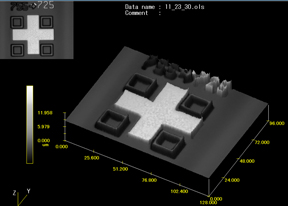
 Olympus Integrated Technologies America, Inc. (Olympus-ITA) has provided an infrared (IR) inspection and defect review system (see figure) with metrology software to SEMATECH for its 3D R&D Center at the College of Nanoscale Science and Engineering’s (CNSE) Albany NanoTech Complex. The system—installed and accepted in April, 2009—enables SEMATECH to verify alignment of bonded wafers and TSV. “We have been collaborating with SEMATECH on inspection and defect review tools since 2001 and working with the 3D group since last year to provide a method to image and measure overlay offsets after wafers have been bonded together,” said Olympus-ITA president Greg Baker.
With so many alliances developing so many technologies, there were so many events during SEMICON West 2009 that it seemed impossible to attend them all. Fortunately, one of the more interesting events was recorded and archived. A panel discussion held both live (for an hour during SEMICON West) and in virtual space (for three weeks, shown as part of PR agency MCA’s “BrightSpots” 3D IC Forum, with excellent text and multimedia links still available online) brought together representatives from SEMATECH, Synopsys, Yole Developpement, EVG, and Terrazon Semiconductor. Paul Lindner, EVG’s executive technology director, offers his viewpoints on the role of wafer bonding and thin-wafer handling with Bob Patti, CTO of Tezzaron, chiming in from the manufacturing side (see YouTube video).
The BrightSpots 3DIC forum was moderated by Francoise van Trapp, formerly an editor with Advanced Packaging magazine, and now working with ex-SEZ technology executive Leo Archer on web-based 3Dincites.com (rhymes with “3D in-sights”). There’s no doubt that 3D is one of the most important technology concepts in ICs today, so it’s great that veterans like Trapp and Archer are working to provide a continuous source of information about this vital direction. –E.K.
Tags: 3D, IC, inspection, interconnect, MEMS, metal, process, R&D, thinning, TSV
