Friday, October 9th, 2009
Founded in 1984 with Flemish government support, IMEC has reached 25 years. To celebrate the organization’s accomplishments, BetaSights joined other industry media outlets attending a research review event in beautiful Leuven, Belgium. From 1999 to 2009 has been the “phase of international breakthrough” as described by current president Luc Van den hove. Working with OEMs such as ASML, in 1999 IMEC installed the first 248nm stepper—the PAS 5000/70—as one of the major sites for beta evaluations; 16 betas (or “pre-beta alpha”) have since been done for ASML. The IMEC Industrial Affiliation Program (IIAP) now works with most of the major OEMs in the world, as seen in the 300mm tools installed in the current fab.
These days, the consortium includes the “largest commitment of semiconductor companies into a partnership,” according to Van den hove. The Government of Flanders has provided steady funding over the years, but the vast majority of the 280M euro budget of FY2008 comes from industrial partners. Including loaned personnel from partners, the total size of IMEC staff is currently 4000.

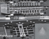
XSEM overview of IMEC’s standard and fishbone cantilever designs with suspended Pt trace and sharp tips (source: IMEC).
In 2000, Philips Corp. decided to consolidate CMOS R&D at IMEC, as the first “core partner.” With the motivation to develop a leading-edge 300mm pilot line, in 2001-2002 the Flemish government funded the start of 300mm fab construction in 2004. By 2005 it was ready, and by 2006 the full set of process tools were installed and other core-partners were attracted. Now a second 300mm line has been funded and is being constructed for official opening in June 2010. In addition, new fab space and personnel are being established to develop photovoltaics, biosensors, and MEMS (see figure).
Having built itself on core technology capability, IMEC now positions itself as provider of advanced system capabilities. The organization is involved in IP generation for configurable RF radio chips, human body sensors and networks, and photovoltaic manufacturing technology. “We are working at IMEC to develop functionalized nanoparticles…which could be used to treat tumor cells. One could also use them for localized drug delivery, which is much better than poisoning the whole body with something like chemotherapy,” said Van den hove.
Continuing CMOS scaling trends, “For 22nm, finFETs are being considered…resulting in better short-channel effects,” explained Van den hove. For extreme high-mobility channels, selective epitaxy of Ge and InGaAs are likely in the future. For memory cells, new TANOS materials (such as GdOx) and cross-bar technologies are also under development.
IMEC works with many universities, and also collaborates with competing international R&D centers such as Fraunhofer and CEA/Leti. SEMATECH’s EUV program dovetails with IMEC’s EUV since both used the “production alpha” tool from ASML, and both organizations have coordinated work on contamination and cleaning of masks and tools. “If there are opportunities, we will take advantages of them; we typically do things in a pragmatic way,” said Van den hove.
Rudy Cartuyvels, IMEC VP and GM Process Technology Unit, presented an overview of IMEC’s process integration capabilities for novel “More-than-Moore” IC applications. Through integrating new materials on the chip, in the chip, and/or below the chip, powerful new functionalities can be developed for volume manufacturing. However, the transition between an R&D site and a high-volume fab often results in delays and unexpected issues. Large and established integrated device manufacturers (IDMs) like Intel and IBM have sufficient resources to handle the transition from IC concept to product reality, but new and smaller companies need help.
With TSMC signed on as a partner (another old Philips tie-in), IMEC recently opened an R&D center in Taiwan. Now explicit connections have been established so that companies can do R&D with IMEC and then transfer production to TSMC for high-volume. “What we are offering with TSMC is a platform to enable the development of innovative product solutions using More-than-Moore technology options,” explained Cartuyvels. “IMEC and TSMC are very complementary; IMEC engages in the development of the technology and shows a functional prototype that is compatible with TSMC manufacturing base.” said Cartuyvels. IMEC has been working with TSMC for many years and there are many TSMC assignees in Leuven.
There are other R&D organizations in the world that offer outsourced process development capabilities, but their unit processes have not necessarily been established in harmony with a high-volume foundry. As the largest IC foundry in the world, TSMC has the deserved reputation for being able to deliver yielding chips built with the most leading-edge process capabilities.
“The whole process is customer driven. Today customers don’t know how there will be a path to high volume manufacturing,” said Cartuyvels. “The engagement of TSMC will depend on the market expectations for the process,” since there is a limitation on how many new technologies the foundry can handle. If the applications remains very niche and low volume then it could remain within the IMEC umbrella. The development phase for IMEC typically ranges from 1-2 years; during that time TSMC can invest in the technology manufacturing capability if they chose.
In addition to the work on system-level-integration and transfer to high-volume, IMEC continues to develop new core technologies for CMOS transistors, metal interconnects, photovoltaics, high-brightness LEDs, MEMS, biosensors, and 3D packages. BetaSights will be covering these developments in future posts. –E.K.
Tags: 193nm, 22nm, 300mm, 32nm, beta, EUV, finFET, Flash, HB-LED, IC, logic, MEMS, PV, SiGe, TANOS
