Tuesday, December 1st, 2009
Based on proven hardware sub-systems from previous models, Applied Materials has released a new chemical-mechanical planarization (CMP) tool that processes two 300mm diameter wafers simultaneously on each of two plattens. Initially targeting copper interconnect formation for memory ICs, the Reflexion GT tool has passed betasite tests at multiple customers, and reportedly provides 60% higher throughput than competing tools while requiring up to 30% less slurry use.
 “Today’s copper-based logic and memory devices have more copper interconnect layers, requiring faster CMP processing and more efficient use of consumables,” said Lakshmanan Karuppiah, general manager of Applied’s CMP business unit. “In addition to its high speed throughput, this new architecture allows customers to realize substantial savings in the cost of consumables, which typically comprises 70% of the total cost per wafer.”
However, we live in a world of trade-offs. In this case, to acheive the lower cost-per-wafer, the tool has only two plattens (see figure) instead of the three found in the company’s previous tools. When establishing a new process of record (POR) for a new line, such as DRAM fabs that are just now transitioning from aluminum to copper interconnects at the 4Xnm generation, it can be cost-effective to start from the beginning with different tools and consumables. For lines already established with three-step recipes that need to add capacity, or for new lines that cannot afford to do more than tweak an old three-step POR, standard three-platten CMP tools will still be required. So these new two-platten tools are really made for new lines.
After planarization is complete, a parallel-path, clean module using proven Marangoni vapor drying delivers highly-effective, water mark-free wafer cleaning. With all of the doubling, modeling a 30k wafer-starts-per-month (wspm) logic fab or a 120k wspm memory fab, Applied Materials claims that seven of these new tools would be needed compared to eleven of “the competition” (presumably Ebara).
How do the consumables costs get reduced? Since the pad is 42” instead of 30”, double the size for double the wafers results in equal pad wear over time, and the larger pad will cost less than double so the pad cost/wafer will improve. Slurry use/wafer is reduced in two ways: lower pad rotation rate reduces the centrifigal force that sluffs it off the edge, and the two wafers share some of the used slurry between them. There is dedicated slurry dispense and pad-conditioning for each head, so that both wafers see the same fresh slurry and pad condition.
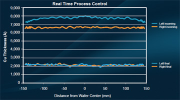
 An insitu eddy-current sensor was used on the prior Reflexion LK tool for within-wafer process control; the sensor’s signal feeds to the Titan Contour wafer holder (“head”) where the back-pressure on the wafer is automatically adjusted. The result is significant improvement in uniformity for each wafer, and the key to the ability to independently control the process uniformity of two wafers on the same platten in the GT tool. The company shows the ability to even “heal” thickness variations between the two wafers (see figure). In today’s fab world of almost vanishingly small process windows, the ability of a tool to reduce the variability of an incoming device structure is truly wonderful. Optical end-point sensors complete the bulk metal and dielectric/barrier process control.
The Reflexion GT system is available now for copper interconnect planarization and has claimed demonstrated extendibility to tungsten applications. This innovative system adds to the company’s decade of leadership in CMP technology, with more than 2,700 systems at customer sites worldwide. For more information, including an animation showing the wafer handling, visit the company’s website. –E.K.
Tags: 4Xnm, CMP, cost, Cu, DRAM, fab, IC, OEM, slurry, tool, W
