Monday, March 8th, 2010
This year’s plenary sessions of the SPIE Advanced Lithography Symposium exposed the complexities of patterning ICs in high-volume manufacturing (HVM) at the 22nm node and beyond. Steppers using 193nm ArF immersion (193i) will be extended using double-patterning (DP) schemes, since the extreme-ultra-violet litho (EUVL) infrastructure is again delayed. R&D to support DP integration has led to the creation of a “Texas two-tone” photoresist requiring only a single developer.
The technical sessions began with a prediction of better times ahead by plenary speaker Kazuo Ushida, President of Nikon Precision Equipment. Ushida noted that the wafer fab equipment industry cleared only $12B in revenue in the terrible year of 2009, but that predictions were for $20B in 2010 with recovery to the 2007 level of $25B by 2011. As usual, the growth in semiconductor revenue will be driven by a Moore’s Law increase in functionality, but achieving that–and particularly the lithography part of achieving it–had become especially difficult. Ushida outlined various possibilities for the future, beginning with a continuation of today’s trend for double patterning using 193nm immersion steppers, some new technology (like EUVL), and stopping the circuit shrink altogether.
Ushida conceded that the EUVL infrastructure was developing too slowly for insertion at the 22nm node. Useable masks might not be available until after 2014 even if someone came up with the $130M needed to develop a mask inspection tool and the defect density of EUV masks and substrates improved 100 fold. To be profitable, a new lithography has to be good for two nodes when introduced, so a tool developed for 16nm node insertion must be useable at 11nm as well. The most likely design for a high volume production EUVL tool then involves a larger numerical aperture (NA) and the compatibility with resolution enhancement technologies (RETs) like dipole illumination. Those RETs, in turn, imply more restricted design rules, such as are being implemented for flash memory today. The higher NA means more mirrors, and an even more powerful source to attain required throughput.
Double patterning, especially using self-aligned spacers to form grating-like-designs, has a natural way forward: the pitch doubled spacers can be used as mandrels for another spacer deposition, perhaps ad inifinitum! The problem is with the cut mask, which defines line ends. Already the cut holes need to be shrunk chemically, but much fancier RETs are coming. Ushida pointed out that extending 193nm lithography in that way would need cost reducing innovations such as tool and mask re-use to remain viable.
The second speaker, Eric Chen of Silverlake Partners, pointed out that future growth was going to be different from the past. In particular, the developed economies have assumed so much debt that they will have to deleverage rather than consume in the coming “reset economy.” Growth, he predicted, would result from increased consumption in emerging markets like China. Developing and manufacturing products for those markets was going to be disruptive for today’s business models. Fast time to market, niche targeting, and low margins would drive the R&D environment. New leaders like Huawei and ZTE would emerge to compete with western technology companies.
Sam Sivakumar of Intel focused on the meaning of these economic changes for future lithography. He deconstructed semiconductor lithography as a play in four acts. In Act1, lithography delivered design intent to the wafer automatically. In Act2, litho manipulations like OPC were sufficient to insure that design intent was realized. However, in today’s Act3, only certain geometries can be printed and thus the designs must be restricted to litho-friendly one-dimensional layouts, etc. In the coming denouement, computational lithography will be required up front to co-optimize proposed layouts, illumination, OPC decoration, and processing.
Thus, Sivakumar warned, the architects of litho design and process must collaborate for success from now on. Further, mask making has become an integral part of lithography planning and cannot be treated as a commodity service. The single biggest future problem would be containing the cost of patterning, he averred.
Complexity increases cost while area scaling reduces it. Sivakumar advocated reducing the number of geometrically complex layers to increase value. He also worried about the cost of EUVL. He warned that EUV masks had to be assuredly defect free as used in the stepper because look-ahead wafers would economically insupportable in any plausible EUVL production scenario. That made EUV mask inspection essential for the success of EUVL and an opportunity for tool vendors to pursue.
Resist and Processing
The keynote talks in the resist symposium were not all about resist. Rather, John Sturtevant of Mentor Graphics began by reviewing the evolution of computational lithography and the models needed to predict resist patterns on the wafer. He emphasized that the algorithms used to apply OPC decoration to a full chip design would always be different from the ones used on TCAD clips for optimization and parameterization. Exotic resist behavior cannot be easily accommodated in models and he wished it could be avoided. At 32nm, a one layer OPC run takes 24 hours on a 400 CPU system, and there are 35 layers now requiring OPC. A modeling accuracy of 1nm is achievable today, he claimed.
Ralph Dammel of AZ Electronic Materials speculated on the chemistries that might be needed for future production. He suggested that planar processing would continue to progress, with graphene eventually replacing silicon as the active layer. The immediate challenge was to do double patterning cost-effectively, though. He outlined several schemes being pursued to avoid an intermediate etch into a hardmask layer, but requiring 6 to 15 steps in the litho cell. None had yet been proved manufacturable, in Dammel’s opinion. Further ahead, Dammel predicted that efforts to develop EUVL resist would break out of the “triangle of death” defined by resolution, sensitive and LER tradeoffs to yield a useful 16nm resist by 2014 or 2015. Before that, he predicted an industry bifurcation where some segments would abandon shrink altogether when optical lithography finally runs out of steam around the 22nm node.
Subsequent speakers described exotic resist systems that might be used in double patterning lithography. Shinji Tarutani of Fujifilm Corp described negative tone resists for 193nm exposure of the sort which could be used for copper interconnect trenches or contacts in a double exposure double etch scheme. Unfortunately the FujiFilm materials required organic solvent development and showed two orders of magnitude less contrast than common positive resists. Still, one had been used at IMEC to pattern 45nm contact holes on a 90nm pitch with 3-4nm CDU.
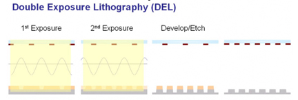
Double exposure in a single resist cannot beat the Fourier optics (k1=0.25) pitch limit if the resist responds linearly, but what if the resist were non-linear in some useful way? Robert Bristol and a team from Lawrence Berkeley laboratories used double exposure experiments to seek out non-linear (non-reciprocal) behavior in potential resist materials. They found a system that produced a photo-base generator when exposed to 193nm light and subsequently flood exposed at 365nm. A second 193nm exposure released the base, allowing development of a pitch less than could be patterned in either 193nm exposure separately. They demonstrated a k1~0.125 but a pitch of 900nm.
Texas Two-Tone
Xinyu Gu and a team from the Willson lab at the University of Texas, Columbia University, and Intel showed a true two-tone aqueous TMAH developed resist for 193nm exposure. A two-tone resist works like a positive resist at low dose, so unexposed material remains on the wafer, but at high exposure it becomes negative-working, so that heavily exposed regions also remain (see figure). Only at intermediate dose levels does such a resist dissolve in developer, which halves the pitch of a properly exposed pattern.
 Gu explained that the Texas Two-Tone resist functioned because it contained a low concentration of photo acid generator and a higher concentration of a lower-efficiency NO2–releasing photobase generator in a conventional CA polymer resin. At low dose, only the PAG exposure mattered and the CA resist was positive. However, once the PAG had all been consumed, increasing dose continued to produce more and more base, ultimately consuming the acid and stopping deprotection and development. A 56nm half-pitch mask resulted in a 26nm line-and-space resist pattern when developed in TMAH.
The Texas Two-Tone resist was termed the most important development in the last 10 years in a comment by Will Conley of Freescale Semiconductor, a recognized industry expert. It does seem more likely to be used in production than resists that require two developers to print both tones: one aqueous and one an organic solvent.
Charles Pieczulewski of Sokudo, a track vendor, explained that tracks were being built for two developers and even two resists for double patterning. Why two developers now? Well it turns out that there is something new in that area as well: 0.26N TBAH, an aqueous base developer that does not diffuse into resin as much as TMAH and thus improves contrast and wall slope while reducing pattern collapse! Adding a solvent developer is not a big step. –M.D.L.
Tags: 16nm, 193nm, 22nm, 32nm, EbDW, EUV, IC, inspection, litho, mask, NIL, RET, reticle, SMO


