Monday, March 15th, 2010
Another back-to-the-future possibility for next-generation lithography (NGL) is direct write e-beam (DWEB), revitalized with multibeam clusters, curvilinear mask writing, and character projection (CP). The E-beam Initiative used the recent SPIE gathering to announce that it had added six new member companies, including GlobalFoundries and Samsung. Aki Fujimura, CEO of D2S and Managing Director of the E-Beam Initiative, announced design for e-beam (DFEB) mask technology from D2S which enables fracturing into circles as well as rectangles, and allows overlapping shapes to create curvilinear features with far fewer e-beam shots.
Since masks are becoming more curvilinear, shot count is exploding for today’s vector systems. Cell projection as promoted by the E-beam Initiative thus appears to be a newly affordable solution. Since contacts always appear round  on the wafer, Fujimura advocates a standard circular aperture for printing contact patterns on masks in one shot, rather than doing OPC with several. The wiggly assist features typically needed for inverse lithography can also be more easily printed with circular or arc-shaped beams, according to Fujimura.
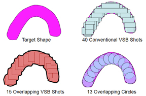
Much of the DFEB value—as presented by Fujimura—lies in overlapping e-beam shots to create better images in less time (see figure). Using conventional, non-overlapping, rectangular VSB shots to achieve this shape, as shown in the upper right, requires 40 VSB shots. By using overlapping rectangular shapes, the shot-count can be improved to 15. However, by using overlapping circular shots, the shot-count is further reduced to just 13 – an almost 70% reduction in shot count over the conventional approach using nonoverlapping rectangles.
Franklin Kalk of Toppan Photomasks highlighted the need to reduce shot count to speed mask production. Today, he said, the capital expenditure for a 22nm mask line is >$100 million, but the output would be one mask/day, without some innovation. It needs to speed up by at least a factor of two to keep 193nm immersion lithography viable for the next 5-6 years.
 Mapper Lithography continues to be the most plausable on-wafer maskless technology, but its progress may be too slow to intercept the 22nm node, and so along with other European programs, it may be re-focusing on the 16nm and 11nm nodes. Still the company proudly announced that a “pre-alpha” demo tool installed at TSMC Fab 12 in Taiwan continues to do R&D work on advanced nodes.
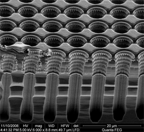
To increase throughput to the required 10 wph level with available technology, Mapper has re-engineered the company’s system to employ a dispenser cathode, at 0.3nA per beam and 7×7 beam parallelism to increase the total dose on wafer to the required 13nA. That results in a considerable increase in complexity as now there are 637,000 apertures, a condenser lens and a beam cross-over in the Mapper system. Still, technology development continues with 7X7 blanker arrays fabricated at 8mm pitch in CMOS using 180nm node fab technology at TSMC (see figure).
Yan Borodovsky of Intel confided to everyone throughout the week that his ideal litho system for Intel-type layouts would be line and cut lithography, with the lines printed using sidewall double (or quadruple) patterning and the cuts probably done using a high throughput EBDW system.
 At the KLA-Tencor lithography users forum prior to SPIE, Borodovsky disclosed Intel’s “rule of thumb” target for the economics of any next-generation lithography approach: US$0.5M in tool price for each wafer-per-hour (wph) throughput specified. Thus, if the tool cost is expected to be $50M then for desired layers the tool must provide 100 wph. With 5KeV Mapper EBDW, to hold to 2nm overlay tollerance the best throughput is probably 1 wph, while loosening the spec to 4nm allows for 10 wph. If the percent exposure is only ~5% for trim, instead of the nominal 50% for most full-field mask layers today, then the relatively relaxed 4nm spec could indeed provide 100 wph.
Borodovsky also shared modeling results for the scattering of electrons into resist to establish reasonable expectations for image blur. Over the 5-50 KeV acceleration range typical for systems considered for EBDW, minimal blur was seen at expected resist thicknesses.
Borodovsky showed data taken by researchers at Technion Israel Institute of Technology in high-k metal-gate (HKMG) transistor damage from 30 keV EBDW, and saw damage due to breaking SiO2 bonds (typically 3-6 KeV bond energy), and slight reduction in dielectric constant (11.7 to 11.5k) resulting in threshold voltage shifts. However, a simple 300°C anneal for 2 minutes in air restores the k to 11.7 by healing the broken bonds. While the ability to heal the HKMG damage is enouraging, we may be safer using some manner of an ultra-thin “charge distribution layer” (CDL), to be integrated with the ARC layer, to shunt electrons away from underlying transistors during interconnect processing.
EBDW for HVM in 2015 still has capability gaps according to Borodovsky: production readiness, wafer defects, throughput, data corruption, and channel-to-channel skew (with thousands of channels). Nonetheless, EUV seems even less capable today and has added mask costs, and some manner of NGL technology will be needed to pattern sparse layouts. Therefore, maskless EBDW may finally reach the mainstream of IC production in the next few years.—M.D.L. and E.K.
Tags: 193nm, 22nm, 32nm, EbDW, EUV, HKMG, IC, litho, mask, NGL
