Monday, April 5th, 2010
The 2010 SPIE Advanced Lithography conference is where we first get glimpses of the future of nano-scale patterning technology for manufacturing. Sometimes, many fuzzy blobs come into focus as a picture in a single moment, and Yan Borodovsky of Intel showed how to do 22nm node litho the day before SPIE officially started. At both Nikon Precision Corp.’s afternoon event, and again at KLA-Tencor’s event in the evening, he showed the tremendous advantages of forcing IC designs into stacks of one-dimensional (1D) patterns.
With optical lithography limited to 193nm illumination and 1.35 N.A. lens-stacks, there are now serious scaling limits in high-volume manufacturing (HVM) of ICs. No matter what source-mask optimization (SMO) tricks are used, the limit to the pitch that can be patterned in a single exposure using a resist with a monotonic relation between dose and development rate is 72nm. Extreme ultra-violet (EUV, at 13.5nm wavelength) lithography is not ready, electron-beam direct-write (EBDW) is too slow, and directed self-assembly (DSA) of molecules remains unproven for IC patterning.
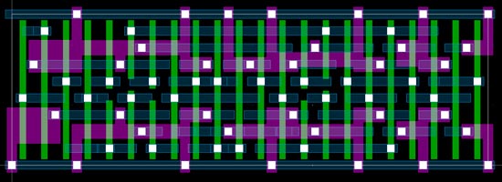
Consequently, it has become more and more expensive to make 2D patterns, and at some point we have to accept the design constraint of strict 1D layouts for logic. While IBM/GlobalFoundries claims to want to keep 2D layouts for logic, Intel began transforming its design intellectual property (IP) from 2D patterns into essentially 1D patterns years ago, and is currently in HVM using lines with a second “cut” mask for logic chips. Sidewall spacer pitch doubling is used for HVM Flash memory today. TSMC is working with Tela Innovations to promote the concept of highly regular layouts; Tela licenses standard cell IP (figure) as well as 2D-to-1D layout transformation services.
Chris Mack, gentleman scientist, provided a wonderful daily blog from SPIE this year, and his February 23 posting summarizes the recent clarity:
“I find it very interesting to see various players in the industry slowly getting behind this basic double-patterning strategy: Designs are restricted to essentially one-dimensional features of a single pitch on a grid. The first patterning step uses 193i with sidewall-spacer pitch doubling that can get the final pitch down to around 38 – 40 nm. A second patterning step then cuts the lines to make the final pattern. The resolution of the second patterning step determines the tip-to-tip spacing of the line patterns, but is a secondary (though important) influencer of packing density. What tool will do the cutting? Immersion with all the optical tricks? Multiple e-beams? EUV?”
To allow for routing connections in logic circuits, the transistors cannot be packed as closely as possible. Generally, compared to the line width, the space between lines is set three times greater. “It turns out that 1:3 is the sweet spot for gratings if you have a low-flare tool,” commented BetaSights’ M. David Levenson. “So long as you can keep the true pitch above 80nm or so, 193i will work for 1-D gratings with one exposure.”

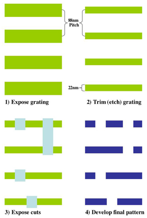
One exposure forms regular dense line arrays, followed by plasma etching to “trim” the linewidths, followed by the second “cut” exposure, to form the final pattern.
For 22nm logic transistor minimum gate dimensions, the first step is to create gratings of periodic and uniform lines and spaces at 88nm pitch. Then a traditional plasma etch tool “trims” a few nanometers from the sides of the lines to form the grating structures with 22nm lines and 66nm spaces. After exposure with the second “cut” mask, the pattern is transferred to the wafer (figure). This fab flow is what allows Intel to enjoy low defect levels and high yields in HVM. Though two patterning steps are needed, the costs are minimized since each step is easier and proper design can expand the overlay tolerance.
Periodic Structures is a new startup-launched with some US government funding-that is trying to create a new exposure tool designed exclusively to form (as per the company name) periodic gratings for the first exposure in this flow. Talking with BetaSights, co-founder Rudi Hendel explained that it’s overkill to use lenses capable of 2D patterning to form gratings, and that they have proven the concept of a significantly less expensive 1D imaging system.
Even with the most efficient “mix & match” exposure tool strategy, double-patterning flows are certainly complex. Former Intel lithography expert Alexander Starikov, current operating I&I Consulting, in a private conversation with BetaSights, wisely noted that all double-patterning schemes actually require three patterning steps for metal interconnect layers! This is because the edges of regular arrays in one IP block generally have to connect with another array or bond pads and somehow non-regular patterns must be formed.
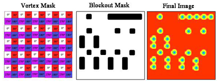
Levenson has identified and long promoted another lithography approach that is conceptually similar to line-cut double-patterning: “Vortex-blanking” double-patterning. Used to form contact patterns, a regular “Vortex Array” mask creates minimally sized dense arrays in a single exposure, to be followed with a second blanking mask to create the final sparse contact pattern for logic (figure). In this method, the phase-shift mask (PSM) structures create the finest spacings possible in a single exposure of a negative resist, and then the block-out mask exposes the ones that you don’t want to print.

Two exposures with Vortex array and blockout (“trim”) mask equalizes CDs across pitch (source: M. David Levenson)
The limit of HVM litho so far has probably been seen in research for the hard-disk-drive (HDD) industry. To get to the smallest possible patterned bit media (PBM), researchers first use EBDW to form sparse posts, followed by DSA of co-polymers to form dense arrays, followed by pattern transfer to form nano-imprint-litho (NIL) master templates with the densest possible 1D structures. Of course, there are essentially no overlay issues with HDD media.
NIL hope for 2D
Perhaps the last best-hope for 22nm 2D patterns comes from NIL. In private conversation with BetaSights, Mark Melliar-Smith of Molecular Imprints Inc. said that his company’s NIL overlay has already been reduced below 20nm in mix and match applications with a 193nm immersion stepper. Data taken at SEMATECH indicates that overlay can be improved with frequent template cleaning or overfill-insensitive alignment marks. At 22nm, Melliar-Smith predicted his company’s jet and flash imprint lithography (J-FIL) technology will have the lowest CoO – neglecting mask cost.
Mask cost and lifetimes may not be a gating factor for the adoption of NIL in HVM of ICs. DNP has already produced 14nm line-space J-FIL masks, according to Naoya Hayashi of DNP. Masks with the 22nm patterns needed for NAND flash in 2013 can now be produced using a 50KV e-beam tool. The etch depth uniformity of 1.8nm is good enough already. However, Hayashi worries that there is no inspection tool for imprint templates, forcing vendors to rely on wafer inspection. Even a new Hermes MicroVision inspection tool will take 32 hours to inspect one field. DNP expects to begin production of replica templates by imprinting the master masks in 2012. Template repair has been proven to work at 32nm, Hayashi reports. -E.K.

