Thursday, February 26th, 2009
One year after this editor covered an SPIE panel on reference metrology and summarized the situation as “there is no more noise; there is only signal,” another lively panel at SPIE this evening discussed the need for not just precise but accurate critical dimension (CD) measurements in advanced IC lines. With smaller structures and reduced process margins, we’re in a era when 2D shapes must be controlled. We can still confidently say that if a 2D shape is within specifications that the process is in control – but how do we know if it is within specs?

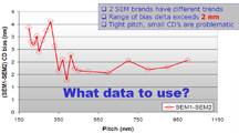
Through-pitch CDSEM bias variation between two brands measuring poly-Si lines (source: Veeco)
Vladimir Ukrainstev, formerly of Veeco and now of Nanometrology International, showed Veeco data on through-pitch SEM bias variation on poly-Si lines from two different SEM brands (see figure). The bias difference can be 4nm, particularly at tight pitches and small CDs. AFM and TEM may aim toward accuracy to resolve the difference, but both techniques are slow and expensive and so some uncertainty in sampling seems inevitable. Audience expert Cyrus Tabery, of AMD and now with “The Foundry Company,” expressed the traditionally pragmatic fab view that precision has always been sufficient.
John Sturtevant, Mentor Graphics litho guru and new SPIE Fellow, said, ”In the old days precision was probably more important because it was easier to measure. The world that OPC engineers live in today has many variables, and accuracy is not what is causing them to fail at 32nm. It’s important, but we’re managing.” For example, he mentioned that we are currently able to get to 90% confidence levels with OPC models, and that’s a small but significant step.
Ofer Adan, CD-SEM expert for Applied Materials, strongly asserted the need for accuracy, “Let’s take roughness as a parameter, we need accurate roughness figures because if we have to figure everything out electrically then we take too much time to get to market.” Hidetoshi Morokama, CD-SEM expert for Hitachi, likewise expressed that we must try to get to accurate numbers for 2D structures despite known challenges. More about this panel and reference metrology will be covered in the next BetaSights Newsletter. –E.K.
Tags: 2D, 32nm, AFM, bias, CD-SEM, IC, metrology
Posted in Equipment, fab, IC, Product | Comments Off on IC reference metrology: small squirrelly signals
Wednesday, February 25th, 2009
Applied Materials’ Technical Symposium at SPIE 2009 featured a panel discussion on next generation lithography (NGL) that was moderated by the company’s Ken MacWIlliams. The outstanding panelists were C. Grant Willson (UT-Austin), Burn Lin (TSMC), Jongwook Kye (AMD), Steve Radigan (Sandisk), and Milind Weling (Cadence). As would be expected from this panel, EUV steppers were not expected to be used prior to 2012. “EUV has gone from if to when to if again,” commented Weling.

Kye reminded attendees that 2012 is just three years from now, and lacking any fab data from which to extract design rules there is no way that designers can plan for chips to be made with EUV. Perhaps by 2015. Of the various options for double-patterning (DP) lithography, Kye sees litho-etch-litho-etch (LELE) as too expensive for mainstream production, so the industry needs to pursue litho-freeze-litho-etch (LFLE) or sidewall-spacer DP (SSDP).
Willson, patterning pundit, commented that for about $100M you can have one EUV tool, or 10 NIL tools sold by his current company, Molecular Imprints. He feels that NIL has the best chance of patterning 22nm features, but acknowledges that mold defect concerns cause hesitation in commiting the technology to production. The many presentations on NIL integration at SPIE this year may have finally cleared the emotional fear that this is just fancy contact printing, so now perhaps someone will try this in an IC fab to get the real defectivity numbers.
Lin promoted bold new ideas in multi-beam direct write and DP. If MEMS technology can produce dense arrays of electron emitters, and said emitters can be stepped or scanned across a field then e-beam could be cost-effective for all critical layers on a chip. For DP, he showed a high-level concept of a scanner to simultaneously expose two masks side-by-side and through optics combine the images into a single pattern.
Regarding the cost of various DP schemes, if your design is for regular memory circuits or logic with gridded-design-rules (GDR) then all of the depositions and etches needed to integrate sidewall-spacer DP (SSDP is a patented variation of self-aligned DP or SADP) are expected to add approximately US$5 to cost per layer. Additional details of Applied Materials’ SSDP flow as detailed by project leader Chris Bencher will be in the next issue of the BetaSights Newsletter. –E.K.
Tags: DP, EbDR, i193, litho, NIL, stepper
Posted in Equipment, fab, IC, Material, MEMS, Product, PV, Service | Comments Off on IC next-generation litho needs all possible tricks
Tuesday, February 24th, 2009
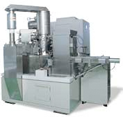
At the Nikon Lithovisions 2009 Symposium on February 22 this year in San Jose, California, Masato Hamatani described the features and beta test results for the NSR-S620 scanning immersion exposure tool, optimized for double patterning lithography. While the tool boasts only one wafer stage, its “Streamlign Platform” concept shoots 200 wafers per hour with 2nm overlay precision after a promised 2 week tool installation time. “The key number is 222,” Hamatani said.
 Achieving such a high throughput without using tandem wafer stages meant speeding up the alignment and metrology steps as well as scan speed. The S620’s (see figure) 5-eye FIA system registers aligment marks in 5 different scribe lines on the wafer with 5 different microscopes simultaneously. The “Stream alignment” system measures wafer height at many places across the wafer with a moving laser beam. Together, these innovations mean that the wafer needs only to be scanned in one dimension through the metrology system (rather than serpentined) before exposures begin.
A dual-stage servo system with four glass scale encoders, many read heads, and a full interferometer in parallel enable a speed of 700m/s with 1ms settling time. The reticle stage acceleration is 12.5 Gs, but the sync accuracy is <1nm (moving average) with <3nm moving standard deviation.
A more complete description of the system will be presented at the SPIE Lithography Symposium this Friday, February 27. The tool is scheduled for first shipment in the fouth quarter of 2009. –M.D.L.
Tags: beta, DP, i193, litho, stepper
Posted in Equipment, fab, IC, Product, Uncategorized | Comments Off on Nikon NSR-S620: Single Stage Double Patterning
Monday, February 23rd, 2009
JEOL will install the first e-beam direct-write-on-wafer (EBDW) lithography tool to support nanotechnology development in the Pacific Northwest when the University of Washington takes delivery of a JBX-6300FS tool. The system will be installed in the state-funded Washington Technology Center Microfabrication Lab. Funding for the tool acquisition was provided through a state-supported STAR researchers’ grant to Michael Hochberg, Assistant Professor of Electrical Engineering, and a matching grant from the Washington Research Foundation.
 In addition to Professor Hochberg’s work in nanophotonics, this tool (see figure) will support nanoscience research throughout the University of Washington and the region. The tool will be available to students as well as researchers from several outside companies whose work includes MEMS research and production/process development. The WTC is the only facility of its type in the Pacific Northwest, offering a publicly-accessible clean room and offering hands on R&D and training support.
This model is capable of writing line widths down to 8nm on substrates up to 200mm in diameter. It is a spot beam, vector scan, step and repeat tool for small volume production as well as “sandbox lithography.” It is also targeted at nano-imprint lithography (NIL) 1:1 mold making, which seems to be gaining in popularity judging from the presentations at SPIE this year. “This is the most flexible, capable machine that you would buy to build nanostructures,” enthused Hochberg.
This new tool joins the one installed n 2007 at the University of Santa Barbara Nanofabrication facility, which is part of the National Nanotechnology Infrastructure Network of the National Science Foundation. There, the going rate is $150 (acedemics) to $450 (industry) per hour for e-beam litho use. They have a wide range of other process tools, and even say they can run the tools for you. –E.K.
Tags: 32nm, 45nm, EbDR, IC, lithography, MEMS, NIL, node, R&D
Posted in Equipment, fab, MEMS, Product | Comments Off on JEOL EBDW litho in MEMS prototyping lab
Friday, February 20th, 2009
As computational lithography has become big big business, the pioneering enterprises have been assimilated into larger organizations (KLA-Tencor for Finle and Synopsys for Sigma-C, to name two examples). Panoramic Technology, however, continues its independence, supplying trustworthy and up-to-date simulators to advanced lithographers for a decade. Past Panoramic products, however, employed an interface that was familiar to users of SPLAT and TEMPEST at the University of California, Berkeley, but seemed difficult to those who had not grown up with it.
 Now, with the new HyperLith simulator, Panoramic believes that that it has created the most easy-to-use and intuitive lithography simulator interface available. Tom Pistor, president and CEO of Panoramic claims even a casual or occasional user can set up a simulation in a few minutes and begin generating accurate and meaningful results. Both the setup GUI (see figure) and the presentation of the simulation output are comprehensive and intuitive, according to Pistor.
True to its roots, the new tool sacrifices nothing in terms of speed, power and flexibility:
*EUV, DUV, immersion capability,
*Kirchhoff or rigorous/TEMPEST mask modeling options,
*Full-vector aerial imaging with polarization control,
*DAIM, or physics-based resist modeling,
*Powerful post-processing, analysis and measurement tools,
*Powerful batching capabilities,
*Distributed computing/parallel processing with SimRunner,
*Full cross-platform compatibility (32/64 bit Windows XP, Vista, Linux), and
*Hardware acceleration available.
Panoramic claims to be selling HyperLith at a fraction of the price of comparable products, maintaining the valued tradition of making computational lithography accessible to individuals, small companies and students. Since the Panoramic simulator stands alone – and is not optimized for any OPC package or style – it can be used as a standard against which faster, but less rigorous algorithms from different vendors can be tested. -M.D.L.
Tags: DUV, EUV, i193, IC, litho, model, OPC
Posted in fab, IC, Product, Service | Comments Off on Independent computational lithography simulator
Thursday, February 19th, 2009
JSR announced today that it has entered into several joint development partnerships (JDP) with IBM to develop low-k dielectrics for 32nm and 22nm nodes of semiconductor technology. The companies will work on next generation materials JSR has had in development and commercial production, including low-k dielectrics and a broad range of photoresists. “This larger scale collaboration is a huge complement to the joint research and development JSR Micro is already doing with IBM in photoresist,” said JSR Micro president Eric Johnson.

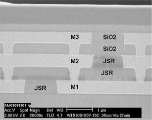
JSR spin-on low-k integrated (source: JSR, credit: K. Mosig)
The companies are working to pave the way for the adoption of three new material technologies: CVD low-k, ultra-low-k (“ULK”, a.k.a. “extreme-low-k” or “porous low-k”), and photo-patternable low-k (PPLK), all developed jointly by IBM Research and JSR Corporation. The CVD precursor is based on a novel molecular structure inspired in part by the spin-on ULK work, and reported offers k=2.2 with reduced sidewall plasma damage, better trench bottom roughness, and better CD control over the process of record CVD low-k material. JSR’s current spin-on low-k (see figure) is not included in the JDP.
The ULK is a spin-on which was originally studied by IBM claiming k<2.0 with extraordinary modulus, toughness to CMP, and purported extendability. While these claims are impressive, a single word reminds us that successful betas may end up losing cost battle: “SiLK.” Despite substantial investment by Dow Chemical in the development of SiLK spin-on dielectric resin to support IBM, CVD remains the low-k technology in most fabs. As cost modeled in 1997 (MRS Spring; N3.10; “Cost-per-wafer of various low-k dielectric integration schemes,” Ed Korczynski, Solid State Technology, Campbell, CA), and since conventionally shown, CVD tends to cost less to integrate compared to spin-on which requires additional bake/stabilization steps.
However, a directly-imageable dielectric with near equivalent final integrated material properties would certainly be a huge cost savings over a mere spin-on. This PPLK material, invented by IBM, cuts several sacrificial materials and their related plasma etching steps, saving costs and reducing process complexity. Details of the PPLK technology will be presented at the upcoming MRS and SPIE Advanced Lithography shows in 2009. The SPIE abstract claims k=2.7 integrated into the fat wire levels of Cu-dual-damascene metallization, with “very high electrical yields using the current manufacturing infrastructure.” –E.K.
Tags: 32nm, Cu, CVD, IC, litho, low-k, porous, resist, spin-on, ULK
Posted in fab, IC, Material, Product | Comments Off on JSR and IBM low-k JDPs for 32/22nm
Wednesday, February 18th, 2009
For thick plating applications like copper pillar bump processing in semiconductor advanced packaging, Shin-Etsu MicroSi has introduced a positive tone, ultra-thick photoresist, SIPR-7126. The 7100 chemically amplified (CA) series has been in production for several years, and the SIPR-7126 has been optimized to reduce processing steps and improve removability in layers up to 100 µm thick. The new material with be shown at the SPIE conference and exhibition, Feb. 24-25, at the San Jose Convention Center in San Jose, California.
This i-line photoresist was developed to plate high aspect-ratio features, like those used in copper pillar processing, and GaAs and MEMS devices. These special applications need an ultra thick layer of photoresist to help cover topography on the integrated circuit and to plate very high aspect ratio features. The material reportedly provides highly vertical sidewall profiles, so that Cu plating can easily form proper pillar cross-sections. The plating chemistries are complex and varied so the resist must also be chemically robust.

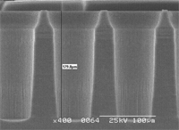
60x180 µm TSV etch; profile angle 70° for top 30 µm, then 88.8° down to 180 µm (source: AlcatelMMS, transferred 2008 to Tegal)
The resist is also applicable to semiconductor etch applications, like MEMS and through-silicon vias (TSV), where process engineers must etch tens to hundreds of microns of silicon to build the device circuitry (see figure). The new photoresist features include:
* excellent flexibility with different plating chemistries, and
* no post exposure bake needed, which allows for
* easy removal and rework.
Shin-Etsu MicroSi, the wholly owned subsidiary of Shin-Etsu Chemical Co., headquartered in Phoenix, Arizona, created this flexible i-line photoresist so that it can be developed by standard TMAH solutions. This new photoresist—which can be coated up to 100µm thick in a single pass—is available for sampling and evaluation now by contacting Shin-Etsu MicroSi. –E.K.
Tags: bump, CA, i-line, IC, litho, resist, TMAH, TSV
Posted in fab, IC, Material, MEMS, Product | Comments Off on Shin-Etsu positive i-line resist 100 microns thick
Tuesday, February 17th, 2009
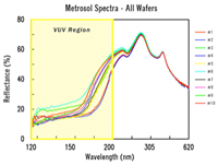
Metrosol has joined SEMATECH’s Front End Process Technologies Program at the College of Nanoscale Science and Engineering (CNSE) of the University at Albany to address metrology and data-analysis solutions for 45nm node and beyond IC fabs. The joint partnership will expand on current work to develop inline metrology techniques to monitor the thickness and composition of high-k (HK) dielectric gate and memory stacks. Metrosol’s vacuum ultraviolet spectroscopic reflectometry (VUV-SR) tool will provide the accurate characterization necessary for inline metrology of advanced logic and memory applications for future technology generations.
“Our VUV-SR technology offers the ability to simultaneously measure thicknesses and compositions of individual layers within the high-k dielectric stacks. Our high throughput provides advanced inline process control capability that allows for greater statistical sampling, more accurate information, and faster problem resolution,” said Kevin Fahey, Metrosol’s CEO.
SEMATECH and Metrosol plan to build optical models for interfacial layers, HKMG stacks, and dielectric capping layers, so that reliable thickness and composition measurements may be performed inline using Metrosol’s VUV-SR technology for different logic- and memory-based applications. Metrosol’s VUV system has already been shown to resolve HfSiOx gate dielectric composition independent of thickness (see figure).
“This is another major step in developing practical and inline advanced physical characterization methods to support emerging technologies currently under development in SEMATECH’s Front End Processes program,” said Raj Jammy, SEMATECH vice president of emerging technology. “Metrosol is a strong, trusted partner, and its VUV measurement technology complements our own technical expertise, as we work together to extend CMOS logic and memory technologies.” –E.K.
Tags: 45nm, fab, high-k, HK, IC, metrology, MG, R&D
Posted in Equipment, fab, IC, Product | Comments Off on Metrosol joins SEMATECH for HKMG R&D at CNSE
Friday, February 13th, 2009
Evident Technologies has announced the issuance of US Patent No. 7,482,059 covering the ability to synthesize a quantum dot with a metal layer which dramatically enhances the brightness and stability of a semiconductor nanocrystal complex. This advance of semiconductor materials science relies on a relatively low-cost colloidal formation processing, instead of needing epitaxial lattice-matching or catalytic growth from wafer surfaces.
 “Since I started working at Evident in 2001, I’ve seen our patent portfolio grow to over 70 patents and patents pending, and it’s very exciting work,” stated Adam Peng Ph.D., Senior Scientist. “This patented material already goes into our LED products that you can buy at local retailers, so even my kids can see the impact our science has on products. I’m proud to be part of the Evident team.” For example, compared to typical white LEDs that are really blue inside of a white phosphor layer, Evident’s “Ice” color Evidots actually emit white light (CIE coordinates X: 0.292, Y: 0.318) directly (see figure). The company reports the luminous intensity for standard 30deg view driven by 20mA is typically 2000mcd.
Evident’s patent calls out a semiconductor nanocrystal core, a metal layer, and a shell, all of which may be grown by the pyrolysis of organometallic precursors in a chelating ligand solution or by an exchange reaction using the prerequisite salts in a chelating ligand solution. The chelating ligands are typically lyophilic and have an affinity moiety for the metal layer and another moiety with an affinity toward the solvent, which is usually hydrophobic. The shell removes surface defects, adds strength, and creates compatibility with a range of matrix materials, organic solvents, and water.
Inorganic colloids have been studied for over a century ever since Michael Faraday’s production of gold sols in 1857. Today, we have metrology technologies which allow for the control of quantum dot morphology and composition on an industrial scale. A spokesperson for Evident told BetaSights that the company uses standard commercial manufacturing tooling, and for LED applications could supply, “100s of millions without further increases in capacity or resources.” –E.K.
Tags: CIGS, dot, IC, III-V, IP, LED, patent, quantum
Posted in fab, IC, Material, Product, PV | Comments Off on Evident quantum dot fab IP
Thursday, February 12th, 2009
CaliSolar is ramping production of upgraded metallurgical-grade silicon (UMG-Si) solar cells and has selected Eyelit’s manufacturing software suite to support its new fab next to its headquarters in Sunnyvale, California. CaliSolar is a private company claiming 15% conversion efficiency from cell made using 100% UMG-Si feedstock that undergoes purification at both the ingot and wafer levels.
Eyelit’s solutions will be used to track material starting with raw silicon and including ingot, brick, wafer and PV solar cell production along with control over CaliSolar’s equipment and other key assets. Eyelit software will provide tool monitoring, management of calibration and preventative maintenance, as well as real-time statistical process control (SPC) and deviation management. PV-Tech has more on information about this new business for Eyelit.
CaliSolar buys MG-Si feedstock and casts ingots, cuts and treats wafers, and manufactures cells. The company is the exclusive licensee of a UC Berkeley patent in UMG-Si that is based on research by CaliSolar founder Eicke Weber, and has filed additional patents covering fundamental methods to purify Si. Using basic materials science principles of thermodynamic stability of phases, thermally-activated diffusion, and gettering of impurities, the company has staked claims to very fundamental principles of UMG-Si fab technology. Since doping, annealing, and etching are standard unit processes that are easily control, the integrated flow should relatively easy to control using Eyelit’s MES.

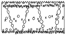
Schematic cross-section of a wafer-based UMG-Si process showing saw-damage and one buried dopant layer to getter impurities prior to etching (source: US Patent Application 20080157241)
Details of the annealing/gettering processes have been disclosed in patent applications. They pull Si ingots out of two-phase melts. Wafer-based gettering at CaliSolar is based on the understanding that wire-saw damage is not a problem but an opportunity. The many defects on the surface act as mechanical getters for bulk impurities under appropriate annealing conditions. Near-surface gettering can be greatly enhanced through the use of sruface dopants such as B, P, Fe or other metals. After annealing, the dopants form a buried region (see figure) below the saw-damage, and etching (presumably wet) ~10µm removes these region to leave behind pure-enough Si for efficient PV cells. CaliSolar could not be reached for comment on the purity increases associated with each of it’s fab steps. –E.K.
Tags: anneal, efficiency, etch, getter, MES, patent, PV, Si, UMG
Posted in fab, Product, PV, Service | Comments Off on CaliSolar UMG-Si PV cells ramping

