Wednesday, February 11th, 2009
At Levitronix’s Ultrapure Fluid Handling and Wafer Cleaning Conference on February 11th, Particle Measuring Systems reviewed the limits of being able to detect things we do not want to find in flowing fluids, as enabled by a new digital detector array they call NanoVision Technology. Steven Verhaverbeke, tool design expert for Applied Materials who presented on particle mitigation concepts in tools, reminded attendees that particles smaller than 30nm are rare both in nature and in fabs, and that most particles are formed as part of processing and so can be anticipated and filtered. This is good since the latest ITRS says that the critical particle size today is supposedly 25nm.

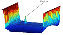
NanoVision Technology detecting a single particle in a fluid (source: Particle Measuring Systems)
Ross Bryant, of Particle Measuring Systems, reviewed the winter 2008 ITRS update and showed that the current specification for ultrapure water (UPW) counts any particles >50nm in size, while any of the various liquid chemicals (including post-CMP cleaning solutions) should be checked for particles >65nm.
UltraChem 40 is the brand name of the new tool that uses the NanoVision Technology. The detector arrays is composed of millions of digital detector elements that wrap around the flow tube to capture the scattered laser light from just a single particle (see figure). The tool can tune into particles while cutting out false signals such as molecular scatter. This all pushes the lower limit on detection to claimed 30nm in UPW and 40nm in chemicals, all with ~5% size resolution.
This new technique could conceivably be used as a large particle counter (LPC) in CMP, too. Since slurry is made of a distribution of small particles, only those >0.5µm count as problems and the digital signal trickery could be used as a high-pass filter to allow for LPC detection. With all of those digital pixels capturing data, there seems to be ample opportunity to extract productive information. –E.K.
Tags: 45nm, analysis, control, IC, ITRS, metrology, particle, spec
Posted in Equipment, fab, IC, MEMS, Product | Comments Off on Plenty of pixels size particles
Tuesday, February 10th, 2009
CMP applications experts gathered in Santa Clara, California on February 10th to share their experience and expertise at the fifth annual seminar sponsored by Levitronix. Leading developers, manufacturers, and end-users of CMP discussed all aspects of the technology, and since Levitronix makes magnetic levitation (MagLev) pumps there were many thorough presentations on slurry distribution issues. While all the presentations were worthy of mention, Budge Johl’s review of slurry particle analysis issues provided an outstanding combination of theory and practice.

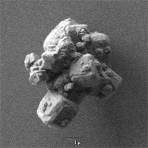
CMP slurry agglomeration (source: Rohm&Haas)
Budge Johl, now with Rohm&Haas Electronic Materials, reviewed the science of CMP slurries and the currently known techniques to monitor fundamental parameters. “Just because we get a number out of a particle analyzer doesn’t mean it’s real,” reminded Johl. He told the tale of finding an inexplicable bi-modal slurry particle size distribution in one fab that eventually could be correlated to a nice single peak distribution in another fab, but not until the same capture times were used in the analysis tools in both fabs.
Instead of tracking the mean particle size, looking at large particle count (LPC) probably provide greater visibility into key CMP issues such as defects/scratches, changes in process performance, or reduced filter lifetime. It is critical to have good training programs and standard operating procedures for preventative maintenance (PM). Johl showed many photos of slurry distribution hardware that was caked with dried slurry due to lack of proper PMs; this dried slurry resulted in extreme LPC in fab CMP tools. “You can see bath-tub rings and stalagtites hangling down inside of day tanks,” said Johl.
With proper care to prevent slurry settling and drying, one of the main causes of LPC is slurry shear induced agglomeration (see figure). However, no good methods exist today to monitor hardness and morphology of particles; in particular, large soft particles may not cause defects so they might realistically be ignored. A new tool to detect particle hardness would be very helpful. Note that Levitronix’s Ultrapure Fluid Handling and Wafer Cleaning Conference runs on February 11th. –E.K.
Tags: analysis, CMP, fab, IC, metrology, slurry, yield
Posted in Equipment, fab, IC, Material, Product | Comments Off on Levitronix seminar shows how to do CMP
Monday, February 9th, 2009
Toshiba claims the prototype of a new Ferroelectric Random Access Memory (FRAM) cell sized at 15F2 acheives read and write speed of 1.6-GB/s using a 130nm node CMOS process. The company will show details of this high bandwidth 128Mb non-volative RAM technology at the International Solid-State Circuits Conference 2009 (ISSCC 2009; Session 27.5) in San Francisco this week. Chips in this family could ultimately be used as the main memory of mobile consumer products, and the cache memory in mobile PCs and SSDs.

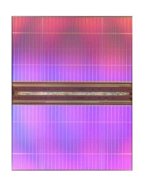
Toshiba 128Mb FRAM (source: Business Wire)
The cell is a re-design of Toshiba’s original chainFeRAM architecture, which was first announced in 2001 as a 30F2 cell of size ~1.9 µm2 using 250nm node technology. Earlier generations of this cell used neighboring data-lines operating in sequence: alternating off lines to provide noise barriers around on lines. By doubling the data-lines at the newer node from four to eight the new cell is just 0.252 µm2, which decreases the total chip area (see Figure). The chip runs on 1.8V, with 83 ns cycle time, and 43 ns access time.
R&D of FRAM technology has been continuous for over 25 years, based on fundamental materials science work on perovskite oxides as the switching layers. It is relatively easy to make a single working FRAM cell in a lab, but it is rather difficult to precisely control the composition of complex trinary oxide thin-films deposited across complex topographies on wafers. Even if you can control the composition properly, the phase can be wrong inside of trenches coated with MOCVD/ALD layers. This is not easy stuff to ramp in a fab.
Chip scaling causes signal degradation as the stored polarization of a memory cell gets smaller. By shortening the data-line pitch in the chain architecture, Toshiba maintained the same cell signal level, and with an improved sensing technique reduced the parasitic capacitance to reach a reading signal of 200mV. Just as parasitic capacitances limit scaling of DRAMs, parasitics limit scaling for FRAMs. The smallest functioning FRAM cell that has been publicized is <10F2, shown by Samsung in 2001, but Samsung’s most recent product announcement in 2002 was for a 32Mb chip using a 0.94 µm2 cell. Some minimal critical mass is needed to hold remnant polarization in useful memory arrays, and so an inherent limit seems to exist for scaling FRAMs. All information on deposition and annealing of switching materials is held secret, so very few people can guess the real scaling limits. –E.K.
Tags: ALD, CMOS, FRAM, IC, memory, MOCVD, non-volatile
Posted in Equipment, fab, IC | Comments Off on Toshiba 128Mb FRAM using 15F2 cell
Friday, February 6th, 2009
The SEMI PV Group today announced the release of its Global Photovoltaic (PV) Standards Roadmap Guidance Document, which identifies immediate opportunities for reducing cost and accelerating innovation in thin-film and crystalline silicon cell and module manufacturing through industry standards. This new roadmap confirms that major manufacturing cost savings are possible through standardizing wafer carriers and physical interfaces, chemical and gas purity, device tracking, equipment metrics, facilities, safety guidelines, silicon specifications, and process controls.
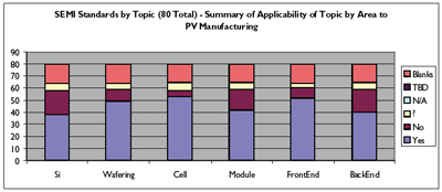
 The Guidance Document provides a high-level assessment of existing SEMI Standards and Safety Guidelines with respect to their applicability to PV manufacturing, as determined by a team of industry stakeholders including equipment and materials suppliers, cell and module manufacturers, and safety experts. Drawing from the 35 years of SEMI International Standards development, over 64 existing SEMI Standards and Safety Guidelines were found that are applicable to PV manufacturing (see Figure). Out of those 64, 31 were rated as ‘Top Priority’ for their potential to deliver immediate cost benefits to the industry with limited or no revisions necessary.
“While many semiconductor equipment, materials, and device manufacturing companies that employ SEMI Standards are diversifying into PV, the PV industry has a highly specialized and unique set of needs, with a diverse set of stakeholders,” said Dan Martin, executive vice president of SEMI PV Business Development and SEMI Global Standards. The Guidance Document further describes planned collaborative initiatives involving other Standards Developing Organizations (SDOs) such as ASTM International, IEEE and others, as well as the increasing participation of research laboratories like NREL (National Renewable Energy Laboratory in the U.S.) and the value of their contributions.
“The next Roadmap development phase will focus on identifying and establishing timelines for the top priority areas in PV manufacturing where new specifications, test methods and safety guidelines will be developed to further reduce the costs of cell and module manufacturing,” said Martin. SEMI is soliciting additional members to join the PV Standards Roadmap Core Team; interested parties should contact Bettina Weiss, senior director, Photovoltaic Segment, SEMI PV Group. –E.K.
Tags: cost, fab, management, PV, Si, solar, standards, thin-film
Posted in Equipment, fab, Material, PV | Comments Off on SEMI PV standards roadmapped
Thursday, February 5th, 2009
Microbridge Technologies, the inventor of passive, analog, MEMS-based precision IC calibration products known as rejustors, announced it has successfully closed an internal round of funding to build out a new presssure sensor family of chips. “The company will launch a line of Micro-Flow pressure sensors that achieve new levels of performance for a wide range of differential pressures,” said Dr. Adam Chowaniec, Chairman of Microbridge Technologies. “With on-chip signal conditioning and amplification, this family of gas pressure sensor chips can address full-scale pressures from tens of Pascal to thousands of Pascal, all with a 0.1 Pascal resolution.”
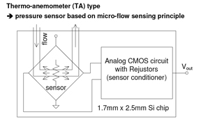
 “No new materials or unit processes were developed,” said Bob Frostholm, Microbridge Technologies vice president of marketing, strategic alliances, and business development. Instead, established 1µm-node unit-processes and materials running at foundry partner XFab have been integrated in a new flow. Since the company’s rejuster is MEMS-based, it is relatively straightforward to imagine combining a rejuster with a pressure sensor as a single-chip (see Figure).
The rejustor uses a polysilicon resistor to heat and modify the grain structure of an adjacent polysilicon trim resistor. University of Freiburg researchers in 2001 reported on the operation and characterization of micromachined CMOS microstructures with integrated polysilicon heaters at temperatures up to 1200K. Also, ST has recently patented an irreversible method to reduce the value of an integrated poly resistor, by subjecting the resistor to a stress current. In all cases, the resistance varies with changes to the poly grain structure; from first principles we know that larger grains reduce resistance, while voids in grain boundaries increase resistance.
Microbridge will sell these new chips in die form to sensor manufacturers, with a full family of products to be announced around the time of the Sensors Expo show in June 2009. The chips reportedly achieve high pneumatic impedances, up to tens of kilo-Pascals, substantially reducing demands on subsequent packaging operations. “The company is sampling selectively now—under strict NDA—and receiving rave reviews,” claimed Frostholm. –E.K.
Tags: CMOS, foundry, funding, IC, integrated, MEMS, pressure, sensor
Posted in fab, IC, MEMS, Product | Comments Off on Microbridge pressure sensor family funded
Wednesday, February 4th, 2009
Allvia, the first through-silicon via (TSV) foundry, has secured $5 million from private investors in a round of funding to expand manufacturing facilities and to build more capacity. After 3 years of revenue generation from providing vertical interconnects and System-in-Package (SiP) solutions, total investment in the company is now $25 million. With in-house processing equipment, a long history of intellectual property (IP) and a fabrication facility in Sunnyvale, California, Allvia offers prototyping services and volume production runs.
TSV are now being designed into many chips, though surprisingly not for the 3D stacking of ICs as many people expected. In an exclusive interview with BetaSights, Allvia CEO Sergey Savastiouk (full disclosure: BetaSights’ Ed Korczynski worked for Savastiouk 10 years ago at TruSi Technologies, but has no current relationship) said that 3D stacking using TSV is not going to happen in mainstream volume anyside soon. Savastiouk mentions issues with reliability, design, and the cost of stacking chips using TSV, and reminds us that it took decades for flip-chip to become mainstream.

Backside TSV bumps (source: Allvia)
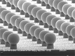
Allvia sees applications for large diameter—defined as >10µm—TSV to be formed using process flows starting from either the backside or frontside depending upon the design. With a portfolio of in-house tools and processes, the foundry can create a wide variety of TSV including dense bumped arrays (see Figure). Allvia is not chasing the elusive market for small diameter TSV targeting 3DICs. “There are two TSV camps today: large and small diameters,” said Savastiouk. “Large is trying to sell today, others are trying to sell into the future.”
Selling today are TSV for image sensors, MEMS, and RF, and most of these count as single-chip and not stacked applications. Passive interposers built with TSV—currently ~1/2 of Allvia’s wafer output—don’t count as 3D stacks and are already in volume production. The company has been active in talking to product people with new devices entering volume production. “There are all kinds of sensors that you have to access from the backside,” explained Savastiouk. Serving a leading technology niche seems like a solid plan. –E.K.
Tags: 3D, foundry, IC, interconnect, MEMS, package, RF, Service, Si, TSV
Posted in fab, IC, MEMS, Product, Service | Comments Off on Allvia TSV foundry adding capacity
Tuesday, February 3rd, 2009
The Collaborative Alliance for Semiconductor Test (CAST) will join SEMI as a special interest group to better manage and accelerate industry progress on critical test issues. CAST expects to gain administrative efficiencies, global resources, SEMI International Standards support, and greater recognition for the CAST agenda. CAST will transfer its governance structure and agenda to SEMI and discontinue operations as a separate non-profit entity, but will continue to try to engage with other industry groups.

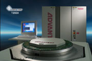
T2000 OPENSTAR-compliant test platform (source: Advantest)
CAST was formed in 2008 by semiconductor device makers and OEMs to work on common industry issues related to test: equipment utilization, lower costs, and greater standardization and ROI on test-related R&D. Charter CAST supporters include (alphabetically): Advantest, Amkor, Infineon, Intel, LTX-Credence, Qualcomm, Roos Instruments, Teradyne, and Verigy. Interestingly, both Infineon and Intel are also members of the Semiconductor Test Consortium (STC)—which aspires to many of the same objectives as CAST—so perhaps the two organizations will somehow be officially aligned.
CAST objectives include:
1. Pre-competitive collaboration on test cost and efficiency,
2. R&D and promotion of international standards (including interoperability) that enable productivity improvements,
3. Benchmarks for quantifying test efficiency and effectiveness,
4. Advocate for a better understanding of the strategic value of test to the industry.
“By joining SEMI as a special interest group, test suppliers and their customers throughout the world will be able to effectively collaborate on pre-competitive standards across company boundaries,” said Don Edenfeld, Manufacturing Test Equipment Development Manager at Intel Corporation, and CAST Co-chair. The advocacy role may be of subtle but significant value, since the value of test itself has often been questioned by naïve designers (and some fab engineers). Particularly in the era of nanoscale structures with inherent systematic variability, test may add more value than any other process step! –E.K.
Tags: group, IC, R&D, SEMI, standards, test, value
Posted in Equipment, fab, IC | Comments Off on CAST as SEMI special interest group
Monday, February 2nd, 2009
Veeco has exited betas with a new Atomic Force Microscope (AFM) named Dimension® Icon™ that provides small-sample resolution for large-samples. Building upon the successful Dimension AFM platform, the latest member of the product line delivers the highest resolution, best ease-of-use, and fastest time-to-results of any large-sample AFM on the market today. “With the Icon AFM, our customers can, more simply than ever, perform analysis ranging from quantitative automated characterization to atomic scale imaging across our core markets of material science, semiconductor, data storage, and energy research,” said Mark R. Munch, Ph.D., Executive Vice President, Veeco Metrology.
 The new tool (see Figure) was engineered to enhance technical performance while simultaneously increasing usability and productivity for users. The system uses a revolutionary XYZ closed-loop head that scans at high-speeds while delivering extremely low drift and low noise. The tool’s temperature-compensating position sensors render noise levels in the sub-angstroms range for the Z-axis, and angstroms in X-Y across the 90µm scan range. This extraordinary performance surpasses the noise performance of most open-loop, high-resolution AFMs. A new high-resolution camera and integrated feedback alignment tools deliver faster probe positioning and sample navigation, allowing users to more easily locate features of interest.
A company spokesperson contacted by BetaSights explained that a lot of innovation was required to make the software as easy to use as possible for non-expert users. The result is a tool that is reportedly much easier to use by experts, too. According to one of the Icon AFM’s beta users, Professor Ralf Seemann of Saarland University, Germany, “The Icon provides high-quality data more easily, and in a shorter period of time, than any other AFM that we have used.”
David Rossi, Vice President and General Manager of Veeco’s AFM Business Unit, commented, “Based upon the excellent reviews that the Icon AFM’s best-in-class performance and intuitive graphical user interface have received from our beta customers, we anticipate broad adoption of this platform in both research and industry. A major goal behind the creation of the Icon was to lower the barrier to entry for high-level AFM research, and to bring this technology into the mainstream of microscopy. We are confident that the Dimension Icon AFM will enable our customers to push the limits of their work.” –E.K.
Tags: AFM, beta, IC, metrology, OEM, PV, R&D, tool
Posted in Equipment, FPD, IC, MEMS, Product, PV | Comments Off on Veeco AFM exits beta with rave review
Friday, January 30th, 2009
Ziptronix wants to help you with your 3D roadmap. The IP spin-out from Research Triangle Park, NC is now actively negotiating licenses to its unique wafer-to-wafer (W2W) and die-to-wafer (D2W) bonding technologies. Using treated-oxide (with surface treatments) and nickel (with a mystery metal) as the connecting materials, room temperature bonding with up to 108/cm2 of 3D interconnects could soon begin with little additional process equipment capital expenditures at IDMs, foundries, and OSATs.

FIB cross-section of InP epi-stack bonded to within 4.5µm on CMOS logic (source: Ziptronix)
According to Ziptronix CEO Dan Donabedian, the company has worked for nearly a decade to be able to deliver the low temperature IC bonding process that is needed to make true 3D IC integration a practical reality today. “We’re currently engaged in substantive licensing discussions with customers in multiple market segments at all levels in the semiconductor supply chain, and we anticipate that several license agreements will be reached in the coming months.”
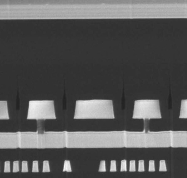
As Phil Garrou summarized last year, Ziptronix low-temperature oxide bonding technology allows for nickel interconnects to copper, tungsten or aluminum TSVs. Donabedian stated, “Because of the depth and breadth of our patent portfolio, we believe that virtually any use of low temperature oxide bonding processes is likely to be covered by one or more of our patents.” The company has already shown the ability to bond InP chips to Si (see Figure).
According to a recent study by Yolé Development, the Ziptronix DBI process was the lowest cost bonding technique when compared to Cu-Cu (copper-to-copper thermal compression) and adhesive technology. In this study, the bonding costs per wafer level (including CMP) were: $57 for Cu-Cu; $22 for adhesive; and just $12 for the DBI technology. The cost savings are due to fast bonding (~2 min. vs. 30-60 min. for Cu-Cu) and no compression being needed so that standard pick-and-place tools can be used. –E.K.
Tags: 3D, bonding, IC, InP, integration, IP, Ni, oxide, Si, TSV
Posted in fab, IC, MEMS, Product, Service | Comments Off on Ziptronix floats IP licenses for 3D IC bonding
Thursday, January 29th, 2009
Aixtron and Ovonyx announced a JDP for Atomic Vapor Deposition (AVD®) process technology to push scaling of next-generation phase change memory (PCM) products. Since it is expected to replace current high-density memory, PCM cells must be made dense and so companies like Samsung (Ref: BetaSights Newsletter 0001) and Numonyx require CVD-like processes for gap-fill instead of planar PVD.
Ovonyx works to commercialize its proprietary phase-change semiconductor memory technology originally invented at Energy Conversion Devices. “Aixtron’s leading market position in thin-film deposition equipment for the semiconductor industry provides an excellent platform for the competitive development of new phase change material by AVD technique for next-generation, high-density confined cell PCM device structures,” said Tyler Lowrey, President and Chief Executive Officer of Ovonyx.

Tricent AVD chamber (source: Aixtron)
AVD is part of the portfolio of vapor-based deposition technologies held by Aixtron that allows for atomic-scale control of functional electronic materials. Aixtron’s exclusive TriJet vaporizer—core technology acquired in 2000—can handle precursors up to 300°C with pulsed injection. The single-wafer showerhead chamber (see Figure) can thus be supplied with a wide variety of precursors, including those with high-viscosity requiring temperatures over 200°C (the typical upper limit for conventional gas distribution systems) for necessary flow.
At SEMI’s SBC this year, Praxair indicated that there are currently ~25 companies proving ALD precursors. IDMs thus have a wide variety of materials to test, and Aixtron’s AVD tool allows for a wide temperature window to not eliminate precursor options. For the distant future, the company is already working with some IDMs on the feasibility of using alternate channel materials (III-V and II-VI) on Si wafers. An Aixtron spokesperson contacted by BetaSights stated that the company has already delivered multiple AVD tools for PCM beta process development to customers. –E.K.
Tags: ALD, chamber, CVD, memory, PCM, precursor, PVD, Si, vapor
Posted in Equipment, fab, IC, Material, Product | Comments Off on Aixtron and Ovonyx partner for PCM deposition

