Wednesday, January 28th, 2009
Silicon Clocks, the developer of custom semiconductor timing solutions that has reinvented itself as a “custom product development house” with a new CEO, has announced a new product based on its CMOS-MEMS (CMEMS) embedded approach. CMEMS-ZeroThermal passive temperature compensation resonators exhibit comparable temperature stability to quartz crystals, while drastically simplifying oscillator design, and reportedly reducing power and circuit size. Company CEO Didier Lacroix told BetaSights to expect more CMEMS technology announcements in the near future.
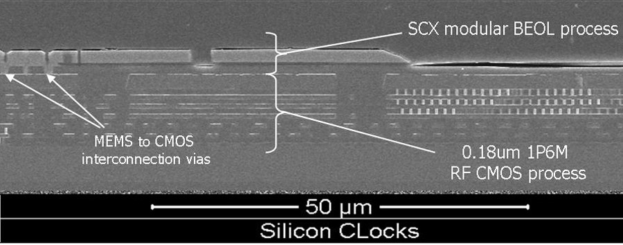
Silicon Clocks has developed a <400°C surface-micromachining flow to create SiGe MEMS, so that these structures may be embedded on chip directly over CMOS metallization (see Figure). The flow starts by making connection to the last level of CMOS metal, much like a redistribution layer (RDL) module:

MEMS resonator over CMOS (source: Silicon Clocks)
1) Connection to CMOS,
2) Deposition of sacrificial Ge,
3) Deposition of 2µm SiGe,
4) MEMS lithography,
5) Sacrificial material removal, and
6) Capping process.
“When you add it all up it’s seven new masks in total; five for the MEMS and two for the cap,” explained Lacroix. “Really what’s different is depositing the SiGe instead of poly.”
Customers could do these additional steps at their existing fab line, or could send wafers post-CMOS to a different line depending upon the volume requirements. Other non-quartz-crystal timing companies—such as SiTime and MobiusMicrosystems—offer stand alone single-chip but not embedded solutions. This technology has reportedly been demonstrated across a wide range of resonator designs from the low kilohertz to several hundred megahertz. Silicon Clocks did their alpha and beta development at SVTC. “SVTC has the capabilities for production, so we consider them to have been our beta,” said Lacroix. SVTC announced major investment last year in 200mm wafer tools to be able to provide a MEMS pilot line, including many tools from SUSS and a Lam etcher.
First-generation MEMS oscillators typically showed 15-30ppm/°C variation with temperature, compared to quartz crystals in the 0.25-1.0ppm/°C range. Matt Hopcroft did excellent Ph.D. work on MEMS resonators, and his 2007 thesis is very worth reading. “Until now, MEMS technology could not compete for ultra-low-power sleep clock applications,” said Lacroix. The company’s completely passive (zero power; no dedicated electronic circuitry) mechanical temperature compensation method is what allows this MEMS technology to match quartz-crystal performance. –E.K.
Tags: clock, CMOS, crystal, integration, IP, MEMS, resonator, Si, SiGe
Posted in Equipment, fab, IC, MEMS, Product | Comments Off on Silicon Clocks embeds MEMS on CMOS
Tuesday, January 27th, 2009
After the 1st “act” of the story of Intel as a memory chip company founded in 1969, the 2nd act really started in 1985 with the decision to bet the company on the 80386 microprocessor according to Richard S. Tedlow, Harvard Business School professor and residential scholar of the Computer History Museum, in a lecture yesterday. The company has been trying to start a 3rd act for some years now, and has decided that independent director Jane Shaw, who joined the Intel board in 1993, will be the one to lead the board of directors when Craig Barrett retires from active management in May.

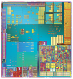
Intel System-on-Chip (source: Intel)
It must have been incredibly frustrating for Barrett at the helm of Intel, leading the most powerful fab capabilities in the world while taking pragmatic risks and executing flawlessly, yet seeing the stock drop >80% from the peak value in August 2000. Tom Krazit at CNET provides an overview on Intel’s recent strategic moves to start a 3rd act, including the >US$1B so far wasted on trying to create new communications chip markets, and efforts in SoC applications (see Figure).
What happens next? Prof. Tedlow is a historian, so to learn from the past he asked Moore and Grove about Intel’s transition to it’s 2nd act. Regarding the critical design win of the Intel 8088 into the IBM PC in 1979, Moore stated, “Any design win at IBM was a big deal, but I certainly didn’t recognize that this was more important than the others. And I don’t think anyone else did either.” Regarding the 1985-1987 launch of the 80386 as a sole-source chip, Grove frankly admitted that while the decisions were more than tactical there really was no new strategy behind them. However, as Grove liked to say, “We earned our luck.”
If history repeats, then what happened to memory chips in the 1990s will happen to logic chips in the 2010s. In part because Intel is sending 90nm logic (specifically not using HKMG technology) to China, we may expect commoditization of logic chips and severe price pressures on current suppliers of MCUs, ASICs, etc. This would reduce profits for any logic chips except HKMG-based microprocessors, so others would find it to be relatively more difficult to fund R&D. Intel might thus gain a lead on developing a new high-volume high-complexity high-profit chip application…but what might that be? “Most companies can’t change,” reminded Tedlow. “For most companies there is no second act.” Any 3rd act will require new technologies—perhaps integrating optics or sensors with electronics—and Intel retains the fab prowess to do groundbreaking work. We’ll see. –E.K.
Tags: 90nm, fab, high-k, HKMG, IC, logic, memory, microprocessor, R&D, SoC
Posted in fab, IC | Comments Off on Shaw to lead 3rd act at Intel
Monday, January 26th, 2009
CEA/Leti, along with e-beam lithography supplier Vistec, and new design and software company D2S, recently announced a collaboration focused on refining and validating advanced design-for-e-beam (DFEB) solutions for 45nm and 32nm nodes. Over the next 12 months, Leti will manufacture test chips using a combination of D2S’ design and software capabilities along with the latest high-resolution e-beam direct-write (EbDW) SB3054 tool from Vistec.

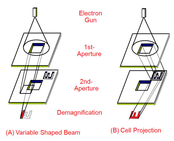
Character Projection (CP) EbDW (source: Hitachi High-Technologies Corp.)
With the cost of advanced mask-sets continuing to increase, direct-write lithography seems essential to allow for low-volume production of custom ICs. EbDW using variable shaped beams (VSB) has been done, but throughput has always been problematic. Character projection (CP) uses standard shapes to convey maximum patterning information in a single e-beam shot. D2S’ software translates the most commonly recurring patterns of chip designs at synthesis into templates on “mini-reticles,” allowing these complex patterns to be replicated in a single CP shot using Vistec’s tool (see Figure). By reducing the design’s required shot count, this approach improves throughput over VSB while enhancing accuracy.
CP itself is obviously a speedup, and making the characters more suitable for the types of designs that might come along can provide a 10-20x increase in writing speed compared to VSB. For a clock-generator or specialized IP there may not be regular characters, but the majority of SoC chips consist of regular blocks like SRAM and I/O that can be made using standard characters. Compared to conventional lithography, assuming $20M/tool for the EbDW tool and 1 wafer/hour writing time and a $4M mask budget, then it is affordable to use CP EbDW for up to 200 wafers according to D2S CEO Aki Fujimura in an exclusive interview with BetaSights.
“If you look at expensive but low-volume products, like high-end cameras or super-computers or FPGAs, if the mask cost can be eliminated and the design-cost is eliminated because it’s a derivative, we can use this technology and serve the long-tail of the market,” explained Fujimura. D2S is also involved in a joint venture with Fujitsu, e-Shuttle, and Advantest, and shuttle runs at Fujitsu for metallization have already started. The work at Leti seems to be focusing more on critical layers. –E.K.
Tags: 32nm, 45nm, EbDR, IC, lithography, node, SoC
Posted in Equipment, fab, IC, Product, Service | Comments Off on CEA/Leti, Vistec, and D2S push EbDW
Friday, January 23rd, 2009
Researchers from Sungkyunkwan University (SKKU) in Korea have found that large graphene films can be formed using CVD over a Ni thin film. The graphene is both strong and stretchy, and at low temperatures the monolayers transferred to SiO2 substrates show electron mobility >3,700 cm2/Vs implying that the quality is as high as mechanically-cleaved graphene. Other researchers have reported >200,000 cm2/Vs by suspending a single layer ~150 nm above a Si/SiO2 gate electrode, but only as a scientific discovery. The SKKU CVD process, developed with Samsung AIT, is the first public disclosure of a possible engineering approach to manufacturing graphene devices.
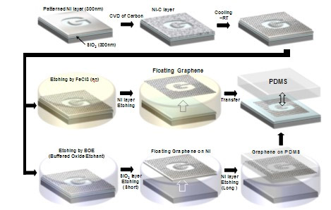
The process flow starts by depositing a 300nm thick Ni layer on a Si wafer. Next, a methane precursor in a CVD chamber at 1000°C followed by a rapid thermal quench forms six to ten atomic layers of graphene. Patterning the Ni layer allows for the creation of patterned graphene for device applications. Two different methods of patterning the films and transferring them to arbitrary substrates have been shown (see Figure).
Prof. Byung Hee Hong, who has been publishing work on manufacturing methods for nanoscale structures since 2001, leads the fabrication work in the chemistry department of SKKU. The lab has the following thin film equipment: e-beam/thermal evaporators, DC/RF PVD, RIE, ion-mill/ICP-etcher, and PECVD and thermal CVD. The crystallographic orientations of the Si wafer and Ni film were not disclosed, but other researcher have reported on the growth of graphene on Pt(111) and TiC(111) surfaces.
Centimeters-wide films that can be bent and stretched without breaking or losing their electrical properties have been shown. The transferred graphene films show very low sheet resistance of ~280 Ohms/square, with ~80% optical transparency. At the upcoming American Physical Society (APS) March Meeting in Pittsburgh, researchers from Purdue University will present information about a condensation technique to form graphene on Ni. Old tricks are being used to create a new material…this all could lead to beta tests of fab processes some day soon. –E.K.
Tags: CVD, electron, film, graphene, IC, mobility, monolayer
Posted in Equipment, fab, IC, Material | Comments Off on Graphene dreams may be real at SKKU
Thursday, January 22nd, 2009
At SEMICON Korea 2009, SUSS MicroTec unveiled the second generation of its ACS300, a modular system for coating, baking and developing of wafers up to 300mm. Compared to the prior generation, the Gen2 tool reportedly costs less, has reduced footprint, and offers configuration flexibility with new capabilities. The system architecture and process modules are specifically adapted to the needs of the advanced packaging and 3D integration industry, which must process up to 100µm thick photo resist layers, and thick films of polyimide, PBO, and BCB.

ACS300 Gen2 HCV module stacks (source: SUSS)
The Gen2 tool was based on a complete platform redesign to reduce the footprint, with a single robot to serve two I/O modules. One process module can be equipped with heating/cooling/vapor-prime (HCV) stacked plates to avoid throughput bottlenecks. The new platform also creates additional space for sub-systems such as pumps, tanks, heat exchangers, and filters so that modifications can be made in the field to adapt to new processing requirements.
“Addressing the specific requirements for wafer level packaging and 3D integration the new ACS300 is equipped with various packaging specific features, which makes it specifically suited for applications like solder bumping, gold bumping or redistribution layers,“ said Rolf Wolf, General Manager of SUSS MicroTec Lithography Division. The ACS300 Gen2 can be interfaced with the MA300 Gen2 proximity mask aligner to form the integrated LithoPack300 cluster.
For 3DIC applications that use thinned silicon wafers, the typically needed “handle” wafer (usually made of silicon or quartz) adds mass that makes handling more difficult. The robot on the new tool has been upgraded to a 6-axis unit that combines high-speed and accuracy, and can handle a payload of up to 5kg such as a multi-wafer-stack or a carrier solution. Since SUSS is a trusted OEM with proven history through the Gen1 tool, the new Gen2 tool has already commanded two orders from customers without first having to show beta data. –E.K.
Tags: 300mm, 3D, IC, lithography, OEM, packaging, tool, track
Posted in Equipment, fab, IC, Product | Comments Off on SUSS out with new 300mm track for 3DIC
Wednesday, January 21st, 2009
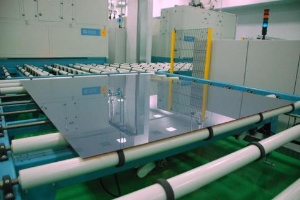
The first customer for an Applied Materials (AMAT) turnkey SunFab thin-film PV fab—Moser Baer in Greater Noida, India—announced today that the 40 MW capacity line has passed final acceptance test (FAT) certification after having met all manufacturing, module efficiency, and yield specifications. PV modules from the line have been certified by the International Electrotechnical Commission (IEC), verifying that they meet stringent performance and safety specifications under challenging environmental conditions.

Moser Baer SunFab line (source: Business Wire)
This beta exit is a major milestone for both companies, since Moser Baer was AMAT’s first SunFab customer. The 40MW capacity line is the largest thin film solar line in India, and uses the world’s largest (2.2m x 2.6m) glass subtrates. “We are excited to see how rapidly this factory achieved 40MW capacity production with high yields—a tribute to great teamwork between the companies,” said Dr. Randhir Thakur, senior vice president and general manager, SunFab Thin Film Solar and Display Business Group at Applied Materials.
Commenting on the development, Deepak Puri, the Chairman and Managing Director of Moser Baer, said: “Moser Baer is pursuing a differentiated strategy in the high growth photovoltaic business and launching production of the SunFab thin film solar module line is of great significance in our effort to bring the solar energy dream to fruition. The thin film line will help us significantly scale up our manufacturing capacity and supply thin film solar modules to our customers. The close relationship we have with Applied has enabled us to quickly ramp up our Greater Noida facility.”
The analysts at iSupply have looked at PV supply:demand balance over the next few years, and predict that overcapacity will result in severe price competition. Vertically integrated companies (such as Moser Baer, with c-Si and CPV fabs in addition to the TF SunFab line) and the most cost-efficient cell lines (such as First Solar) should fare the best during the anticipated shake-out. Overcapacity in module production will exceed 160% in 2009 and remain above 100% through 2012, bringing silicon module prices crashing down to between US$2.50 and US$2.75 per watt. –E.K.
Posted in Equipment, fab, Product, PV | Comments Off on AMAT SunFab exits beta at Moser Baer
Tuesday, January 20th, 2009
Just over five years ago, I was one of the steering committee members of the MIT • Stanford • UC Berkeley Nanotechnology Forum, and had the pleasure of meeting new U.S. Energy Secretary Steven Chu when he was one of the presenters at our first event, “Nanotech beyond the hype,” held May 29, 2003 at Stanford University.
Seeing the potential for nanotech to be hyped even back then, the forum was held to look at the current state-of-the-art in nanotechnology applied to energy, health, information, and other human needs. Providing the pragmatic perspective of a benchmark from nature, Chu showed how human ear cilia have evolved to provide excellent frequency response and automated signal gain, and that humans haven’t even begun to understand how to try to improve upon this design. He showed a unique ability to communicate complex technical topics with clarity, so we may hope that he will be highly effective in directing national policy.
“Simply stating, in my opinion,” Senator Dianne Feinstein of California, said, “there is no one brighter or more equipped than this man to become secretary of energy.” After the hearing, even environmental groups that oppose coal and nuclear plants praised Chu’s commitment to renewable fuels and efficiency. Having been director of Lawrence Livermore National Laboratory, Chu’s opinions about renewable energy technologies like photovoltaic (PV) are on the record. He seems pragmatic and focused, and we need that type of energy leadership now more than ever.
PV fits into the portfolio of renewable energy technologies that includes wind, wave, biomass, and geothermal. All of these technologies seem to have advantages in one location or another, and all seem worthy of funding by the DOE. We may be thankful that NREL has been dutifully working on all aspects of PV technology development for decades, and that some of that work is now ready for production in partnership with HelioVolt. –E.K.
Tags: energy, PV, R&D, solar, technology
Posted in fab, PV | Comments Off on Energy Secretary Chu good for PV
Monday, January 19th, 2009
Posted in Uncategorized | Comments Off on MLK Day observed
Friday, January 16th, 2009
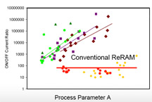
At SEMI’s SMC yesterday, Sung Wook Park, executive vice president and general manager of Hynix Semiconductor, provided a keynote address on the materials needs for mainstream memory chips over the next decade. DRAMs will likely turn into STTRAMs, and NAND Flash will probably be replaced by ReRAM (Ref: Ed’s Threads 080505). Combinatorial materials R&D company Intermolecular claimed to have leaped over the rest of the world in finding an ideal materials set for ReRAM.

Combinatorial materials R&D led to a new ReRAM with >100 ION/IOFF (source: Intermolecular)
Using a three-stage screening process, Intermolecular tested over 75k conditions over a 20 month period to discover and optimize ReRAM; >4k different cells were tested which generated a lot of IP. Flash specs are 10k cycles, while most ReRAM tested so far reaches only ~1k cycles. “Moved to an entirely new materials set, and the result of that was a behavior that is fundamentally different,” explained CEO David Lazovsky. The new materials reportedly meet ION/IOFF>100 (see Figure) and endurance >10k cycles.
When will this new materials set be needed in production? Technology node progression for memory will soon slow down. DRAM scales to ~32nm, and then a completely new technology such as spin-transfer torque (STT, a.k.a. tunneling magneto-resistance, or magnetic tunnel junction) RAM would be needed by 2012. NAND should scale to ~22nm using floating traps, then cross-point ReRAM should work. Phase-change memory (PCM) may also work soon. “The PC RAM has a slight lead, but the ReRAM is gaining a lot of interest,” declared Park.
Tradeoffs are inherent in our era. 8F2 DRAM cells had been the standard, but most companies have already moved to 6F2 cells (based on a “twist” structure). Scaling in DRAM has already led to extreme aspect-ratios (AR) for storage capacitors; >45 for 4xnm node technology, so a tradeoff has been the need to physically link them for mechanical stability. Single-wafer and dry cleaning technologies help in the processing of such extreme structures. Innovation is needed now more than ever before. –E.K.
Tags: DRAM, Flash, materials, memory, MTJ, NAND, PCM, R&D, RAM, ReRAM, SMC, STT, TMR
Posted in Equipment, fab, IC, Material, Product | Comments Off on Hynix sees STTRAM and ReRAM some day
Thursday, January 15th, 2009
 As SEMI’s SMC today, Raymond Roberge, SVP and CTO of Praxair Electronics, proposed a pragmatic new collaboration model for electronic materials R&D. Semiconductor fab process materials TAM for 2008 was ~$10B, yet materials suppliers now question their ongoing profitability. “Certainly the 300mm shift has resulted in productivity advances for IDMs at the expense of materials suppliers,” asserted Roberge.
Electronics (incl. IC, PV, FPD, LED) gases are ~8% of Praxair’s $11B sales. For other large materials suppliers, electronics typically are 1-10% of sales. These companies are positioned to be able to exit the IC fab business if it no longer makes sense, unlike OEMs that typically are utterly dependent upon this market.
If suppliers drive R&D, there are high costs and inefficiencies (like the 25 ALD precursor suppliers who chased $50M TAM last year), while if an IDM drives R&D then disclosure limitations lead to single source supply (like Rohm&Haas who still holds >90% of CMP pad SAM [source: Linx Consulting]). Collaboration models must be adjusted for mutual profitability:
• Early selection of limited suppliers (one or two materials companies),
• Detailed disclosure of requirement (with one or two OEMs),
• Supply/purchase commitments by the IDM, and
• Cross licensing to “share share” (so that IDM receives dual supply, and suppliers receive ROI).
Speaking with BetaSights after his presentation, Roberge acknowledged that there have been collaborations between materials suppliers and IDMs, and between materials suppliers and OEMs, but the industry needs to move to a more sophisticated model where all three are brought together. While such collaborations have been considered in the past, the difference this time around is that the materials R&D costs and risks remain high, but the former high growth potential is gone. “The industry needs to look at appropriate value sharing, so that materials companies can have a reasonable expectations of earnings throughout the cycle,” said Roberge. –E.K.
Tags: 300mm, ALD, CMP, electronic, fab, IC, IDM, materials, OEM, R&D, SMC, supplier
Posted in fab, FPD, IC, Material, MEMS, Product, PV | Comments Off on Praxair’s materials R&D collaboration model

