Wednesday, January 14th, 2009
Smart Equipment Technology (S.E.T.), a wholly-owned subsidiary of Replisaurus Technologies and a leading supplier of high accuracy die-to-die (D2D), die-to-wafer (D2W) bonding and nanoimprint lithography solutions, announced yesterday that it will collaborate with IMEC on 3DIC R&D. IMEC’s 3D integration program explores 3D technology and design for applications in various domains, focusing on 3D WLP and 3D stacked-ICs to find innovative solutions for the cost-effective use of 3D interconnects.

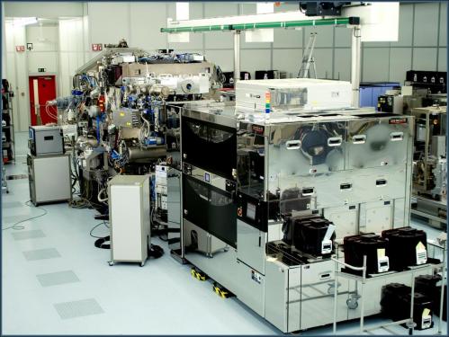
S.E.T. FC300 bonder inside (source: S.E.T.)
S.E.T.’s automated FC300 flip chip bonder will be used in the joint development program to work on die pick-and-place and bonding processes for 3D chip integration. With more than 250 tools installed worldwide, from semi-automated for R&D through automated for production, S.E.T. bonders flip both fragile and small chips onto substrates up to 300 mm. The FC300 is spec’d with accuracy of 0.5µm, and capable of applying high force (4,000N).
The program is scheduled to begin during the first quarter of 2009, at which time S.E.T. will enter IMEC’s Industrial Affiliation Program (IIAP) on 3D integration. The parties will collaborate to develop both pick-and-place and bonding processes, which are required by advanced 3D integration schemes. “The Replisaurus and S.E.T. technologies are very interesting for advanced packaging applications, and the integration of this tool in particular will help complete our program,” said Luc van den Hove, Executive Vice President and COO of IMEC.
“IMEC’s installation of the FC300 is fully in line with Replisaurus’ product and technology portfolio, which offers game-changing opportunities to the global chip market,” said James Quinn, CEO of Replisaurus. Replisaurus is selling a tool to do ElectroChemical Pattern Replication (ECPR) for integrated passives, copper pillars and TSV. When I met Quinn two years ago, his vision was to develop the full infrastructure needed to bring ECPR to production. Phil Garrou provides an excellent overview of ECPR in his recent blog at SI. While this process is still in beta evaluation, the principle of low-cost micron-scale (instead of nm-scale) patterning is unquestionably the right solution for advanced packaging. –E.K.
Tags: 3D, bonder, chip, ECPR, flip-chip, IC, integration, interconnect, JDP, stacked
Posted in Equipment, fab, IC, MEMS, Product, Service | Comments Off on Replisaurus 3DIC R&D with IMEC
Tuesday, January 13th, 2009
At SEMI’s Industry Strategy Symposium (ISS) running at Half Moon Bay, California today, IMEC president and CEO Gilbert Declerck talked about the need for R&D to facilitate IC industry growth. An industry based on answering the question, “what have you done for me lately?” can never rest on past successes and must continue to innovate. Even in difficult economic times, major technology investments are needed to keep up with evolving customer expectations. IMEC’s “open innovation” R&D model has resulted in the organization being able to show electrically functional 0.186µm2 32nm SRAM cells using EUV for contact hole patterning.

ASML EUV demo tool interfaced with TEL Clean ACT12 track in the IMEC 300mm fab (source: IMEC)
The two ASML EUV full-field tools delivered to IMEC and Albany Nanotech in 2006 were termed “alpha demo tools.” Normally, any tool delivered to a customer fab for evaluation counts as a “beta,” but in this unique case the tool really is still in alpha. The EUV source itself is still under development, and the rest of the tool is not based on the latest production hardware. ASML has announced five orders for the first “NXE” EUV production steppers, and we may expect that the first units shipped will be considered as beta evaluations.
IMEC works on both CMOS scaling (more Moore) and novel devices and system integration concepts (more than Moore). Heterogeneous integration may include any of the following technologies:
• SoC, Sensors, Actuators using 130nm CMOS (200mm wafers),
• SiGe MEMS,
• RF//mixed-signal using BiCMOS
• 3D SIP, WLP, and RF integrated packages, and
• Si nano-photonics.
IMEC continues to attract participants from IDMs, OEMs, materials suppliers, and increasingly from fabless companies like Qualcomm. IMEC has grown to include over 1700 staff members, of which nearly 600 are visiting assignees from partner organizations.
As we start the new year, it’s good to reconsider the big picture of all of the new work we have ahead of us. ISS continues tomorrow, followed by SEMI’s Strategic Materials Conference (SMC) at the same location. I’ll be there. –E.K.
Tags: 32nm, 3D, ADT, CMOS, EUV, fab, IC, investment, lithography, MEMS, Moore, R&D, SoC
Posted in Equipment, fab, IC, MEMS, Product, Service | Comments Off on ISS growth theme set by IMEC
Monday, January 12th, 2009
Rudolph Technologies today announces Discover Solar™—the first fab management software tool designed specifically to help photovoltaic (PV) manufacturers increase cell efficiency and reduce costs. Discover Solar accepts all available data from each step in the solar manufacturing process, and then applies statistical process control (SPC) algorithms to generate automated reports. A company spokesperson confirmed that the product is in at least one beta evaluation, and has hit production targets.

Sun (source: umbra.nascom.nasa.gov)
While retaining the Discover brand name used for IC yield software, this new offering is substantially different. Mike Plisinski, vice president and general manager of the company’s Data Analysis and Review Business Unit explains, “Discover Solar incorporates a completely re-engineered database structure and analysis engine optimized for the unique requirements of high-volume photovoltaic production. It provides comprehensive analysis of process performance information, allowing manufacturers to discover and act upon opportunities to improve the energy conversion efficiency of their products. Using Discover Solar, PV process engineers can monitor the health of a complete production line and quickly identify tool and sub-component problems as well as incoming material issues.”
The process control software suite performs tasks including automated root cause analysis, statistical process control, equipment performance and history tracking, and advanced charting and report generation. Designed to support high-volume PV fabs running over 50,000 cells per day, the software can also assist in identifying 2nd-order effects between tools and processes, and in catching incoming material quality excursions. Discover Solar is available now for purchase.
Aaron Hand at SI provides a fine overview of this technology, including mention that Rudolph got the core IP in the 2006 August merger, and August acquired it from Inspex. KLA-Tencor acquired the “wafer inspection” assets of Hamamatsu Photonics subsidiary Inspex back in 2004 when August got the “data management” assets. With PV fabs running orders-of-magnitudes higher volumes compared to IC fabs, targeted technology like this from Rudolph makes a lot of sense. –E.K.
Tags: control, excursion, fab, management, MES, PV, quality, software, SPC, yield
Posted in fab, Product, PV, Service | Comments Off on Rudolph’s PV fab management software
Friday, January 9th, 2009
SolFocus, the Mountain View, California developer of Concentrator Photovoltaic (CPV) systems, today announced that it has raised $47.5 million in the first close of its Series C financing and appointed Mark Crowley chief executive officer. Crowley, who was named president of SolFocus in August 2008, will assume the role of CEO, while previous CEO and founder, Gary D. Conley, will continue as chairman of the board. The company aims to grow CPV deployments from 0.5 MW in 2008 to approximately 100MW by the end of 2010.
 Crowley noted that this first close comes despite what is one of the most challenging funding environments in history. “Many good companies are going unfunded today; this close is strong validation from investors that our CPV systems are compelling today, and will help drive the growth of the solar industry tomorrow.” The SolFocus CPV design employs a system of reflective optics to concentrate sunlight 500 times onto small, highly efficient solar cells (see Figure). The SolFocus 1100S system is claimed to achieve >25% efficiency, using triple-junction III-V PV cells from Boeing subsidiary Spectrolab. In solar-rich regions of the world, CPV panels integrated with advanced tracking systems may soon reach levelized cost of energy (LCOE) parity with fossil fuels.
Last fall, the IEEE silicon valley chapter of the electron devices society (SVC-EDS) and Applied Materials co-sponsored a PV Tech Symposium in Mountain View, California, where Russ Jones of Spectrolab presented an overview of the company’s triple-junction technology. Spectrolab runs a Ge substrate fab in Sylmar, California that is scaling up from 100mm to 150mm wafers to allow them to fab more concentrator PV (CPV) cells in two weeks than the entire installed capacity today! CPV systems today represent only ~10 MW of global supply, but Spectrolab plans to bring capacity online by 2010 to represent ~250MW/year of power under 500X concentration.
Spectrolab currently produces its second and third generation of lattice-matched triple junction cells, starting from a Ge wafer as the substrate and bottom cell, a Ga(In)As middle cell (after a buffer layer), and a GaInP top cell. These structures demonstrate 37.5% and 38.5% efficiency, and the company’s next generation “metamorphic” triple junction should show 40% efficiency. A four-junction “inverse metamorphic” cell, with the wide-bandgap layer grown first off of the Ge, is claimed to ultimately lead to 43%.
A new Veeco E475 MOCVD reactor has been installed at the Sylmar fab, which is the first step in the conversion to 150mm diameter Ge wafer processing by 3Q10. Most of the tools in the new line will be used, allowing for significant cost-savings. Nearly all 150mm wafer process equipment was designed with robotic handling and sophisticated process recipe control by the OEM, providing greater control and generally improved yields. So Spectrolab should be able to deliver the volumes needed by SolFocus over the next few years. –E.K.
Tags: 150mm, concentrator, CPV, Ge, III-V, LCOE, MOCVD, PV, solar, SolFocus, Spectrolab
Posted in Equipment, fab, Product, PV | Comments Off on SolFocus gets new money and new CEO
Thursday, January 8th, 2009
Samsung has launched a new press release for “super-thin LED monitors” (http://www.businesswire.com/news/home/20090107006252/en) that are really LCDs with LED backlight units (BLU). The company’s new P2370L is just 16.5mm thick and uses white LED instead of cold cathode fluorescent lamp (CCFL) illumination. Compared to CCLF units, LED BLUs consume 30% less energy, are constructed without mercury, and allow for monitor thickness reduction. The LED BLU is claimed as the reason that the monitor has a 2M:1 contrast ratio, and reproduces more vibrant colors with higher contrast ratios than other monitors, at a $399 MSRP. The P2370L display will ship in late 1Q09.

White LED backlight unit (BLU)
These white LEDs are manufactured by combining blue-emitting InGaN chips and a suitable fluorescent converter. So not only is this “LED monitor” not an LED monitor, but strictly speaking, the light from the LED chip itself is never seen. What is seen is the emission from the excited white phosphor layer (after being filtered), which is not conceptually different from the white phosphor layer inside a CCFL found in a standard LCD display.
Samsung has been working on white LEDs for at least 12 years, since Aixtron delivered MOCVD reactors for this application to Samsung in 1997 (Ref: http://www.aixtron.com/press/semi01.htm). In 2008, Aixtron reports excellent MOCVD business for high-brightness LED applications (http://www.semiconductor-today.com/news_items/2008/AUGUST/AIXTRON_080808.htm).
In addition to it’s internally developed technology, Samsung has also received licensed technology from Osram GmbH, the lighting company based in Munich, Germany. In 2004, Samsung entered into a royalty-bearing license agreement with Osram to manufacture and sell white LEDs using Osram’s patented conversion technology. Osram has also signed a patent cross-licensing agreement with Nichia, and also licensed its white LED technology to Rohm, Everlight, and Lite-On (http://compoundsemiconductor.net/cws/article/news/19101).
Greater volume of white LED manufacturing should continue to lower prices. Eventually the world will move to all LED lighting (http://www.pennwellblogs.com/sst/eds_threads/2008/01/080121-smc-highlights-pv-led-and.php?dcmp=WaferNEWS_ARCH), and the light bulb will be the last vacuum tube component to be made obsolete by a solid-state device. –E.K.
Tags: backlight, BLU, FPD, InGaN, LCD, LED, lighting, MOCVD, Osram, Samsung
Posted in Equipment, fab, FPD, Material | Comments Off on Samsung LED backlighting proliferates
Wednesday, January 7th, 2009
On January 6, 2009, ASM International and SAFC Hitech (a business segment within SAFC, a member of the Sigma-Aldrich Group) announced that they have entered into a certified manufacturer and partnership agreement for ALD precursors for barium- and strontium-based high-k insulators. The agreement includes certification criteria, a license to certain ASM ALD patents, and a partnership for marketing and further R&D.

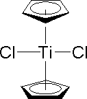
Ti cyclopentadienyl precursor (Source: SAFC Hitech)
Finnish researchers Vehkamaki et al. showed the use of cyclopentadienyl precursors for the “Growth of SrTiO3 and BaTiO3 Thin Films by Atomic Layer Deposition,” in Electrochemical and Solid-State Letters, 2(10):504-506 (1999). So the basic idea has been around for a decade, waiting for the real need that is now here with 32nm node memory production.
I did early R&D work on BaSrTiO3 MOCVD precursors in 1995 (knowing we were far ahead of the curve), and one of the inherent problems was the control of stoichiometry in final films, due to competition by MO precursors for the oxygen in the deposition chamber. ALD processes may avoid this problem if the Ba and Sr are in separate layers. Otherwise, the SAFC Hitech folks will have to engineer one large molecule to carry both the Ba and Sr in proper proportions (http://www.mrs.org/s_mrs/sec_subscribe.asp?CID=2618&DID=116023&action=detail).
“SAFC Hitech has been working closely with ASM’s research groups for some time, focusing on evaluation and process development of this class of cyclopentadienyl source materials,” commented Dr. Peter Heys, Research and Development Director, SAFC Hitech. I’ve toured their facility in Sheboygan, WI (http://www.pennwellblogs.com/sst/eds_threads/2008/04/080429-safc-hitech-opens-modular.php) so I know that they’re up to the challenge one way or the other. –E.K.
Tags: 32nm, ALD, CMOS, cyclopentadienyl, DRAM, high-k, HK, IC, MOCVD, precursor
Posted in fab, IC, Material, Product | Comments Off on ASM and SAFC Hitech to work on Ba and Sr ALD
Tuesday, January 6th, 2009
The first issue of the BetaSights Newsletter has been published (see link to a free copy in the right-side column of this page under “Newsletters”), and a reader has already provided a correction. Michael Current (San Jose, California) noticed that the initial web-link to the slides from Prof. Asenov’s IEDM 2008 variability presentation was incorrect; the correct address is http://www.elec.gla.ac.uk/groups/dev_mod/presentations/Asenov_IEDM_08.pdf to access all 25MB of in-depth information.
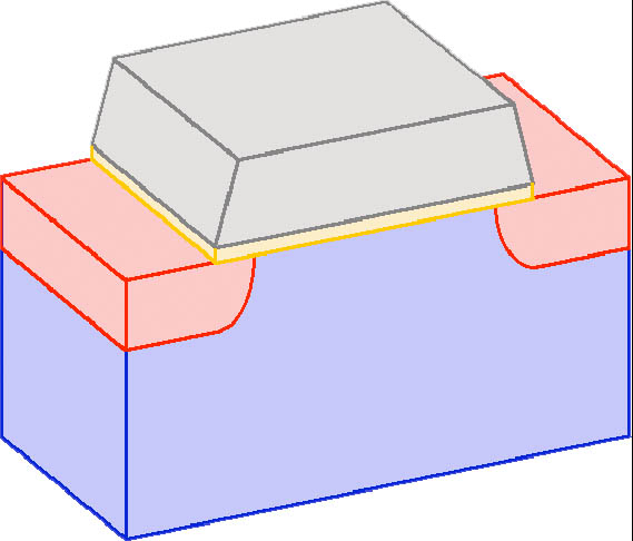
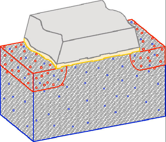
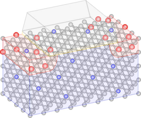
 As Current commented about this presentation, it is rare to find a set of slides that so thoroughly explores the leading-edge of fab technology, and even more rare to find a set that does so without obtuse mathematical equations. For example, slide #6 in this set shows three images for MOSFET transistors (see Figures to the right): the top for a modeled ideal transistor, the middle for a 22nm node device, and the bottom for a 4.2nm MOSFET. You can clearly see the granularity of matter at 22nm, which explains why statistical variability is inherent at this scale.
 Looking at the 4.2nm rendering, everything is so chunky that it’s difficult to even try to draw a line to define where one region ends and another begins. At the risk of getting philosophical, even concepts like “junction” or “barrier” seem to lose meaning at this scale. Chips need to operate near room temperature where there is sufficient energy (ekT) to make things move around, but even if atoms didn’t diffuse (in a hypothetical alternate universe) it still seems impossible to extend current fab technologies to make devices this small.
 Though we may have seen the limits to CMOS shrinks, some of us still want to move to 32nm and 22nm node processing. People are contemplating these moves with an understanding that new ways of working will be needed. As Asenov concludes, “Statistical variability demands a statistical approach to design and will force fundamental changes in the design paradigm.” –E.K.
Tags: CMOS, IC, node, scaling, shrink, variability
Posted in fab, IC, Service | Comments Off on Very variable transistors
Monday, January 5th, 2009

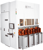
FSI ORION modular single-wafer cleaning tool
FSI International, Inc. (Nasdaq: FSII) announced December 23, 2008 that it has received an order for it’s new ORION® single wafer cleaning platform after a beta evaluation by a major semiconductor manufacturer. The tool will be used for resist strip in 32nm metal interconnect modules, using FSI’s proprietary “ViPR” extension of the classic “piranha” (a.k.a., sulfuric-peroxide mixture or “SPM”) chemistry.
FSI has been pushing the envelope with wet cleans for many years, and I’ve talked with CTO Jeff Butterbaugh many times about this application. Generally speaking, interconnect cleans have always allowed for more material losses than transistor cleans, and so had been considered as “less critical.” Being less critical, single-wafer process control was not considered as essential, so batch tools have dominated interconnect cleans. However, ever reducing process margins, material loss and galvanic corrosion in copper interconnects now suggest single-wafer control.
“This order is important to us on many levels,” said Don Mitchell, FSI’s president and CEO. “It validates the critical capabilities of the ORION for 32nm applications. It also demonstrates this customer’s conviction that those capabilities add sufficient value that even in a deep industry down-cycle, manufacturers are willing to invest in innovative technology, not only to prepare for the future, but also to realize current gains.”
The tool incorporates many of FSI’s core technologies: in-line chemical blending and control, energetic aerosol chemical and water delivery, and recipe-driven procedures. Its modular design accommodates multiple chamber types and permits the addition of modules to increase maximum throughput. The ORION’s unique closed-chamber design also permits the use of volatile, highly-reactive chemistries for single step, all wet stripping of the highly implanted photoresist created during the fabrication of 32nm devices. By eliminating ashing, it not only reduces material loss but also decreases the cycle time, process complexity and the number of tools and process steps. –E.K.
Tags: 32nm, beta, clean, interconnect, Semiconductor, single-wafer, SPM, ViPR
Posted in Equipment, fab, IC, Product | Comments Off on FSI cleaning tool exits beta with payment
Sunday, January 4th, 2009
This is the first example of a posting to BetaSights new BetaBlog. New posts will appear most working days, so bookmark this site and check back regularly.
BetaSights was founded in the fall of 2008 by industry veterans Ed Korczynski and Elizabeth Schumann, to provide commercial free, member supported, productive info about fab beta sites. Before an IC, FPD, MEMS, or PV technology can move from alpha R&D into commercial production, it must be evaluated at a fab beta site to prove fit for an application. It is these critical materials, equipment, and services that BetaSights tracks.
The BetaSights home page will soon include a Sights table of beta information. Basic information will be free for anyone to access without registration, while additional in-depth information will be available for members-only access.
Tags: Equipment, fab, FPD, IC, materials, MEMS, PV, Service
Posted in Equipment, fab, FPD, IC, Material, MEMS, Product, PV, Service | Comments Off on Welcome to the beginning of BetaBlog(SM)

