Monday, July 19th, 2010

Two of the biggest original equipment manufacturers (OEM) supplying semiconductor fabs have released new etch chambers that are tuned for the selective removal of mere monolayers. Applied Materials just announced a new “Mesa” field-retrofittable upgrade to it’s “AdvantEdge” ICP etch chamber, targeting several challenging new applications. Tokyo Electron provided an update to applications plans for the Radial Line Slot Antenna (RLSA) chamber first announced in March of this year. Both tools have reportedly passed

SEMI CEO Stan Myers opens Intersolar 2010

SEMI CEO Stan Myers opens Intersolar 2010

beta-site tests, as this editor mentioned in his invited talk at the NCCAVS Plasma Applications Group meeting, held July 15 this year on the floor of SEMICON/West-Intersolar (figure).

Single-wafer etch chambers have historically been designed for maximum etch rates to deal with microns of material, starting from the first etcher released in 1979 by Tegal (still supplying tools {Thanks to Tegal vice president Paul Werbaneth for the invitation to present at the NCCAVS-PAG}).

From the 1981 release of the Lam AutoEtch 480—featuring atmospheric loadlocks and fully automated recipe control—to today’s tools handling 45nm CDs, maximum etch rate has always led to greater throughput and thus to better Cost-of-Ownership (CoO). However, for 45nm node and below ICs, Dennard Scaling in support of Moore’s Law has led us to device structures where critical materials are now measured in terms of monolayers. The result is an opening in the market for process chambers that are specifically designed to etch as little as a single layer of atoms across 300mm wafers.

However, we are specifically not considering the use of true atomic-layer etch (ALE)—conceptually similar to atomic-layer deposition (ALD) where reactants first adsorb then react and byproducts somehow finally sublimate—for chip manufacturing yet. Nor are we considering the use of neutral ion-beams which can remove atomic layers but generally lack selectivity to underlying materials. At present, it seems that we only need to extend legacy etch chambers with new sources and recipes to be able to meet current needs. How needy are we these days?

Perhaps the most challenging etch need today is for high-k metal-gate (HKMG) transistors used in 45nm and below CMOS ICs, where work-function altering oxides of aluminum and lanthanum are less than 1 nm thick. Since the gate is the heart of the transistor, any variation in etch profile across the wafer directly results in final device variability, and so as a rule of thumb we must control the etch to 10% of thickness…less than a single atom.

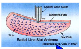
Originally developed for satellite broadcasting, RLSA has been explored as a plasma source by Tokyo Electron for many years (figure). Work at the Tokyo Electron Technology Development Institute in Hyogo, Japan has been led by vice president and general manager Tosh Nozawa. In an exclusive interview with BetaSights, Nozawa-san explained that the 2.45 GHz RLSA source demonstrates the unique ability to provide uniform etching across an extraordinarily wide pressure range: from 5 mT up to 5T.

(US Patent App. Pub. No. US 2008/0142159 A1)

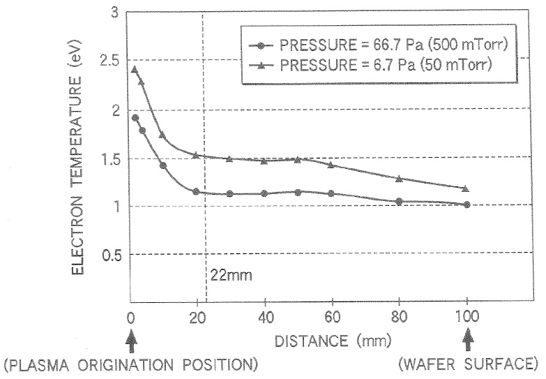
RLSA etching provides relatively high densities of radicals decoupled from the electron temperature (figure). The wafer is not completely “downstream” from the plasma, so anisotropy can be maintained with bias. However, the electron temperature can be as low as 1 eV at the wafer surface, and TEL reports minimal charging damage on sensitive test structures compared to legacy sources.

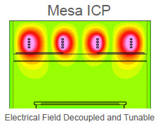
Applied Materials has found a way to extend a legacy inductively-coupled plasma (ICP) source with two complementary techniques: additional source-coil complexity, and an innovative way to synchronize pulses to both the source and bias powers. Standard ICP source coils have been split in two, which allows for cross-chamber tuning of the electric field (figure). The result is better control of etch rate over the 300mm wafer surface, and the ability to fine tune within-wafer uniformity.

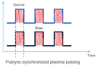
More innovative is the new source-bias sync (figure) that provides superior within-die uniformity. When power is off during the cycle, there are several significant local uniformity benefits:

  • charging on the etch mask has time to dissipate,
  • byproducts inside recesses have time to exit, and
  • reactants have time to refresh surfaces inside recesses.

Also, the duty cycle can be adjusted to seriously slow down the process to handle monolayers. “For example, the etch rate can be tuned down to one Angstrom/minute using chlorine plasma,” claimed Thornsten Lill, Applied Materials’ vice president of etch technology development, in an exclusive interview with BetaSights. Compared to a continuous-wave plasma that over-etches 4nm, the synchronous pulsing over-etches <1nm.

Applied Materials reports that the combination of the split ICP source with source-bias-sync significantly improves the depth uniformity when there is no etch-stop, such as in shallow-trench isolation (STI) and buried word-line (bWL) etches into silicon. The company claims 1% silicon etch-depth can be maintained across 300mm wafers, and <1 nm (3 sigma) CD for lines/spaces. Where the use of a continuous wave source would result in measurable non-uniformity in etching trenches, the pulsing source reduces the non-uniformity by 2/3.

TEL has provided the forward-looking-statement that 20 chambers are expected to be sold in the first year, for applications in both transistor and interconnect formation. Applied Materials has provided the backward-looking statement that it has shipped >60 chambers over the last 6 months to etch both metals and silicon, and that the hardware changes can be field-retrofitted in a single production shift. Based purely on end-user demand, it is likely that other OEMs will release new or significantly upgraded plasma etch chambers, and the market for soft plasma etchers will be very dynamic for the next few years. “The more selectivity you have in the etch the more flexibility you have in the overall integration,” said Uday Mitra, Applied Materials’ vice president and chief technical officer of etch, in an exclusive interview with BetaSights. For process development and integration, these new etch capabilities are very welcome additions to the metaphorical tool-box.E.K.

Monday, July 5th, 2010

With the world now manufacturing nanoscale ICs and MEMS, new devices require the formation of thin-film coatings from exotic material precursors. Atomic-layer depostion (ALD) as an extension of chemical vapor deposition (CVD) technology can be used to form both dielectric barriers and metal connections. With a tool designed to deposit almost any thin film, French OEM Altatech Semiconductor S.A., has recently received orders for ALD/CVD systems that will be used for the R&D of 3D and high-mobility ICs.

In May of this year, the Fraunhofer Research Institution for Electronic Nano Systems (Fraunhofer ENAS) in Chemnitz, Germany, ordered an AltaCVD system (figure) from Altatech to deposit advanced silicon stressor materials on 200mm wafers. Silicon stressor materials are used to increase the channel mobility of transistors, enabling higher processing speeds.

Fraunhofer ENAS is scheduled to install the new AltaCVD system in its back-end-of-line (BEOL) cleanroom facility in Chemnitz during the second quarter. A previously installed system is being used to deposit diffusion barrier and copper layers for advanced copper damascene interconnects and through-silicon-via (TSV) features.

“After evaluating Altatech’s innovative technology and its AltaCVD equipment, we have ordered a system for our lab, where we’re developing nanometric thin films to advance the state of semiconductor processing. The use of liquid-phase precursor injection and evaporation is a key enabling technology for this work,” said Prof. Stefan E. Schulz, head of back-end-of-line operations at Fraunhofer ENAS.

Altatech also won an order by Fraunhofer IZM’s new All Silicon System Integration Dresden (ASSID) group for a 300mm AltaCVD system. Just opened on 31 May 2010, the ASSID is specially designed for projects in 3D wafer-level system integration (200/300 mm) and prototype development for manufacturing partners in industry. As part of the Fraunhofer IZM Institute, which specializes in transferring IC advanced packaging and system integration research results to industry, ASSID is integrated into a technology network of applied research institutes and universities.

The equipment is scheduled to go online in the third quarter of this year at ASSID. The site’s Class 1,000 cleanroom is equipped with a complete 300mm wafer fabrication line for TSV formation and post-processing on both the frontside and backside of wafers, wafer thinning, 3D device stacking, and package assembly and testing. ASSID will use the AltaCVD system to create through silicon vias (TSV), processing both standard and thin silicon wafers. The low-temperature AltaCVD tool will deposit stacks of film layers and ultrathin, conformal isolation layers inside deep vias and trenches with aspect ratios as high as 40:1.

In addition to handling either 200 mm or 300 mm wafers, AltaCVD’s flexible architecture allows it to be used in volume production for plasma-enhanced deposition (PECVD) of dielectric materials, stacks and metal films as well as in R&D for metal-organic processing (MOCVD) in back-end-of-line (BEOL) applications such as creating direct-platable barriers.

Altatech Semiconductor’s AltaCVD platform uses direct injection of liquid precursors and an advanced flash-vaporization system in processing wafers up to 300 mm. The modular system can accommodate a wide range of vaporization and deposition temperatures, enabling users to select the optimal process windows for their specific applications, which can include deposition of advanced materials for high-k gate dielectrics, metal gate electrodes, capacitors and 3D integration. For thermal CVD or RF-enhanced deposition steps, a low-frequency plasma enables tuning of the thin film’s mechanical, electrical and optical properties.

“Through our partnerships with Fraunhofer ENAS and other leading research centers, we are continuing to develop liquid-precursor deposition processes for high-k/metal gates, through-silicon-vias, memory and capacitor applications,” said Jean-Luc Delcarri, president of Altatech Semiconductor. “We’re also working with IDMs and foundries to bring liquid-precursor deposition to their high-volume 300 mm fabs. And we’ve begun applying our CVD technology to create advanced thin films for solar cells, high-brightness LEDs and other microelectronics markets.”

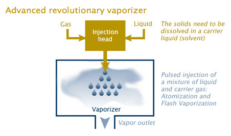
Key features of Altatech’s low-pressure injection (LPI) vaporizer (figure):

  • Improved atomization, due to carrier gas “blasting” the flow into claimed 5-40µm droplet diameter range with maximum population at 10µm (compared to 6 to 60µm with max population at 22µm for high-pressure direct injection),

  • Longer droplet residence time inside the vaporizer due to low liquid pressure (2 to 5 bar), and

  • Sequential or co-injection from 2-4 injection heads provides for binary or higher order alloy deposition, and the ability to form nano-laminates in a single-chamber.

With the above capabilities in the source injector, the company claims that the system can work with any of the following liquid precursors:

  • TEOS,

  • n-octadecyl trimethoxysilane,

  • glycidil methacrylate,

  • n-hexadecane,

  • III/V precursors (TMGa, TMAl, Cp2Mg, etc.), and

  • Proprietary organometallics (Cupraselect™ for Cu, Chorus™ for Ru, etc.).

Diluted solid precursors such as ß-diketonates, Alkoxides, and proprietary molecules can also be vaporized by the system.

“Through our partnerships with Fraunhofer ENAS and other leading research centers, we are continuing to develop liquid-precursor deposition processes for high-k/metal gates, through-silicon-vias, memory and capacitor applications,” said Jean-Luc Delcarri, president of Altatech Semiconductor. “We’re also working with IDMs and foundries to bring liquid-precursor deposition to their high-volume 300 mm fabs. And we’ve begun applying our CVD technology to create advanced thin films for solar cells, high-brightness LEDs and other microelectronics markets.”

No deposited film exists independently, and the smaller the device structure the tighter the integration required. Films that play an active role in the device function—such as high-k metal gates (HKMG) for 32nm node CMOS ICs—must be carefully integrated with various physical and electrical barrier layers. High-volume manufacturing (HVM) necessarily changes as little as possible, and so any new material must always fit into old flows, and any new tool must be proven as reliable.

Liquid-precursors have always been challenging to handle in CVD systems: bubblers tend to lack precision, and vaporizers generally lack reliability. Vaporizers have been used for decades, yet nozzles still get clogged, and interior walls still build-up particle contamination. Encouragingly, in an email exchange with BetaSights, Altatech claimed that it’s low-pressure injector design allows for 6 months of “production mode” use between preventative maintenance (PM) cleanings of the vaporizer.–E.K.

Wednesday, June 16th, 2010

While most of the IC manfacturing world has embraced the fabless/foundry split between design and manufacturing, Intel has remained staunchly vertically integrated and continues to reap the rewards. At the recent 2010 International Interconnect Technology Conference (IITC) in Burlingame, California, researchers from Intel confirmed that the design constraint of a fixed spacing between interconnect lines allows for the use of “air-gaps” in manufacturing to increase circuit speeds. While this approach has been considered for over 20 years, today no other company has all of it’s logic chip designs converted from anything-goes 2D to strict 1D layouts. Consequently, no other IC company can easily use this low-cost manufacturing trick today, even though EDA startup Tela Innovations has been selling gridded-design-rule (GDR) IP for a while now.

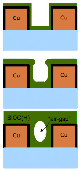
CVD can be easily tuned to initially coat sidewalls (top), then pinch-off (middle), and finally form a closed pore (bottom) during one step.

With shrinking IC sizes, the dielectric insulation between metal interconnects has become one of the major limits on increasing circuit speed, so the last 15 years has seen relentless pursuit of ever lower capacitance (“k” value) dielectric materials to replace SiO2 glass (k~4.0). Sadly, there are many devilish details of materials integration into nanometer-era ICs, and one by one the dozens of possible new low-k materials failed to meet specifications: too leaky, too soft, too unstable, and too expensive. The history of this debacle can be read in the wishful thinking specification for low-k dielectrics found in successive versions of the International Technology Roadmap for Semiconductors (ITRS) from 1998 to 2008. In 2010, with a few very limited exceptions, the only low-k dielectric used in commercial fabs is CVD SiOC(H) with k~3.0.

In fact, CVD SiOC(H) is such a good dielectric that nearly all attempts to reach k<2.5 now use this material as part of the final structure. Empirically, it has been found that nanometer-scale pores can be created in SiOC(H), and such porous low-k (PLK) films can get to ~10% porosity for a k~2.7 without too many problems. However, aiming for lower k-value generally results in connected pores that make soft and leaky and unstable films, and the work-arounds add expense and uncertainty. Still, as shown at IITC, most fabs are still pursuing work-arounds to strengthen, stabilize, and cap PLK films. In contast, Intel has chosen to add a single central pore to SiOC(H) so get to lower k (see figure).

To be clear, there is no “air” in what is not really a “gap” in an air-gap; it’s more like vacuum inside of elongated holes. Intel has developed an air-gap process that uses no new materials, and requires only dry 193nm lithography for one additional masking step:

  1. Standard Cu dual-damascene interconnect formation,

  2. Mask using 2x minimum CD (allowing for dry 193nm),

  3. Etch out dielectric (preserving via landings and wide areas),

  4. CVD of a conformal dielectric liner, and

  5. CVD to partially fill and “pinch-off” the top openings of the gaps.

Note that, despite repeated questions from the audience, the Intel presenter refused to say which materials are used for the two final dielectric, nor the final effective k-value of the structure.

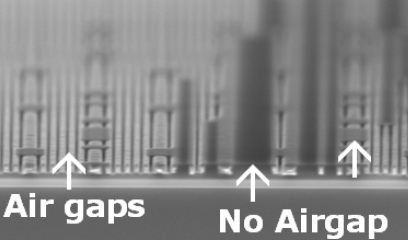
32nm node IC interconnect structures showing air-gaps (source: Intel)

However, the company disclosed that for the tightest-pitch interconnect layer (56nm for both lines and spaces) on 32nm node test chips (see figure), a >20% reduction in the effective capacitance was achieved with air-gaps. Moreover, the company claims that 22nm node test chips show ~28% capacitance reduction compared to full SiOC(H). While the specific dielectrics used were not disclosed, from known films we can guess likely scenarios. The pinch-off dielectric is almost certainly SiOC(H), since any other stable material would have k>3 and would increase the effective k too much. The conformal CVD film could be SiOC(H), or SiO2, or even SiC since the k value of a liner would add relatively little to the final effective k.

The lithographic masking step is needed for two reliability reasons. First, by excluding air-gap formation in areas near next-layer vias, alignment between layers can be more easily done. Second, wide spaces are excluded where the final non-conformal CVD step wouldn’t automatically pinch-off to close the gaps; leaving full SiOC(H) in wider spaces also helps with mechanical strength. The next layer is patterned with a conventional daul-damascene flow, with the option to add air-gaps.

Dry 193nm litho used to mask off areas that will not be converted to air-gaps (source: Intel)

Dry 193nm litho used to mask off areas with no air-gaps (source: Intel)

With the masking step to improve reliability and lifetime (see figure), and with etch and deposition optimization, Intel claims that air-gap pilot manufacturing yield for 32nm SRAM tightest-pitch layers is similar to the process-of-record (POR). The company tested dielectric breakdown and thermo-mechanical packaging issues with various air-gap integration flows, and found that the proper combination of barrier layers allowed for equivalent results to the POR. The quality of the interface between the conformal CVD dielectric and the metal is important. Also, the quality of the metal barrier must be good to eliminate fast diffusion paths that could induce unacceptable levels of electromigration.

Perhaps the most significant claim of this new interconnect process flow is that no new failure modes were reportedly observed. In contrast, PLK process flows to get to >10% porosity use new materials and new process steps that almost always combine to produce new ways for the integration to fail, which is another reason that PLK dielectrics have so far failed to replace SiOC(H).

Remembering that Intel is the company that Andy Grove built, and that Grove wrote the book entitled “Only the paranoid survive,” it remains reasonable to consider mildly paranoid theories about the company’s motives. In particular, history has shown that next generation technology announcments can sometimes be deliberate mis-directions: publishing detailed maps that just happen to omit known dead-ends. Intel has not said it will ever use air-gaps in production. All the company has said is that it could use air-gaps in production with good results. Since it is the only known IC company with 1D logic designs ready to go, it could happen for 22nm node manufacturing.

Thorough coverage of IITC this year has been provided by industry expert and Techcet analyst Mike Fury, who attended the full conference including the short-course. Fury’s wit often equals his wisdom, even if he has pony-tail envy. –E.K.

Thursday, April 22nd, 2010

HP Labs in Palo Alto has been leading the development of the “memristor,” and researchers there have finally discovered the underlying mechanism for the formation of devices that can function as memory cells, logic circuits, and potentially even real artificial intelligence (AI)! Disclosing these results in his plenary speech to the attendees at the Nanocontacts and Nanointerconnects Workshop at the Spring 2010 Materials Research Society meeting on April 5th in San Francisco, HP Labs group leader Stan Williams (figure) explained how to make memristors without use of the hitherto-uncontrollable “electroforming” step.

Stan Williams (source: HP)

Stan Williams (source: HP)

At the risk of oversimplifying, a memristor can be thought of as a complex oxide sandwiched between two metal contacts, where the electrical resistance of the oxide changes due to current-flux induced ion drift that forms conductive filaments. Memristors were famously predicted in theory in 1971 by Leon Chua of U.C. Berkeley (Ref: IEEE Trans Circuit Theory 18, 507-519; 1971), yet theory provided no clues for practice, and it was only in 2008 that the Williams Group proved the function in oxides of titanium. “Leon Chua is the Albert Einstein of circuit theory,” declared Williams.

One of the biggest problems with HVM of memristor circuits had been that PVD of pure “rutile” (TiO2) titania results in simple resistors. Before these simple static resistors can become dynamic memristors, they have to be “electroformed” using a strong voltage-current applied for a minimum time. Electroforming was known to induce movements of ions and defects in the oxide, but we did not really know what final structure was created, and so could not begin to control the process so as to be able to integrate it into a complete device HVM flow.

“We spent ten years messing around making all the wrong measurements and coming to all the wrong conclusions before we discovered that these things are memristors, and we had to do time-dependent measurements,” explained Williams.

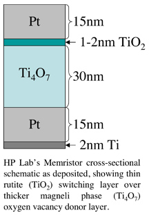
Williams’ Group at HP finally went through great expense and effort, networking with U.S. government labs for access to nanoscale materials characterization tools, to dissect memristors pre- and post-electroforming to determine what was happening at the atomic level. They found that electroforming was reducing the rutile TiO2 to a single-crystal of “magneli phase” Ti4O7 under each contact. For large area contacts, the Ti4O7 always appeared like a ~100nm diameter nanoscale plug relatively independent of the contact area, since essentially all the current flowed through this one plug during electroforming.

At geometries near optimal for memristor function, a 1-2nm thin TiO2 layer remained as a tunnel barrier. The width of the tunnel barrier then changed by ~0.5nm by the movement of ions within the oxide during memristor function. The switching mechanism for the memristor is thus field-induced drift of positively charged O+ vacancies in TiO2 that controls the resistance of the film. The Ti4O7 functions as a source/sink of O+ vacancies to diffuse into and out of the TiO2. “This can be thought of as a condensed phase of vacancies in TiO2,” according to Williams.

With this new understanding, Williams’ Group was able to conceive of forming the final device structure without having to electroform. Sourcing a new Ti4O7 PVD target, they now sputter 25-30nm of Ti4O7 followed by 1-2nm of standard TiO2 between ~15nm thick Pt electrodes (figure). To avoid oxidation of the bottom Pt electrode, they discovered that a few nm of Ti deposited below the electrode provides sufficient Ti to diffuse through the Pt and pin any vacancies at the Pt/Ti4O7 interface.

Other oxides sandwiched between other metals can also become memristors. Tradeoffs in materials selection involve switching speeds, device lifetimes, and manufacturing costs. While HP has led the world in pursuing memristor technology using the Pt/TixOy/Pt stack, there has been a rush of global R&D in both academia and industry to explore other materials systems. Indeed, there were dozens of papers presented at the Spring MRS Meeting on devices based on ionic transport in oxides to controllably change the resistance, however all of the presentations seen by this editor included mention of electroforming as part of the manufacturing flow. While additional materials engineering is needed to create high-yielding memristor arrays in high-volume manufacturing (HVM), it looks like everyone now has to agree upon two facts:

•    from a HVM perspective, non-electroforming is the only way to go, and
•    from a design perspective, memristors are intrinsically dynamic devices.

Memristors for ReRAM
HP Labs has been working on the smallest possible memory elements using cross-bar architectures. At the types of fields you can put on a nanoscale device you have to be concerned with the potential for damage at contacts. Argonne National Lab is testing some of the HP Labs’ newest 20nm line/space crossbar structures, but it is not easy to push the limits of the nanoscale manufacturing. For example, impedance spectroscopy is not so useful, because in non-linear devices the whole concept of impedance is not even valid.

Despite the difficulty to dynamically measure memristors, now that they are not-so-difficult to make we can use static properties to make memory arrays. With the ability to switch the resistance quickly between relatively high and low static states, we can make random-access memory (RAM) cross-bar array circuits with densities that beat Flash for equal minimum critical dimension on chip.

The main limitation now holding fabs back from making high-yielding ReRAMs is probably the Pt electrodes. So far, noble metal contacts seem to be essential to prevent contact oxidation and parasitic resistances, and noble metal patterning generally requires “lift-off” integration which can be problematic in geometries smaller than several microns. Still, lift-off is easily controlled for larger geometries, and the use of sidewall spacers and sacrificial masking layers may allow for high-yielding extendibility to <20nm and smaller devices.

Memristors for logic
There is an ongoing need to be able to create ever faster devices that can “flop” as elements of logic circuits. As Ghavam Shahidi of IBM Research in Yorktown Heights, NY presented at the “Device Architecture: Ultimate Planar CMOS Limit and Sub-32nm Device Options” short course at IEDM 2009, the world now has the ability to create 12.64 TeraFLOP ICs, with ExaFLOP ICs imagined by the year 2020. Extrapolating today’s state-of-the-art planar CMOS IC parameters out to ExaFLOP requirements, the power consumption would be 100s of MW to a few GW (for reference, a nuclear reactor typically produces ~1GW). Massive memristor arrays could theoretically provide high-speed logic functions with dramatically reduced power consumption compared to CMOS.

Since the memristor is a dynamical device, it changes with time, and two equations are needed to describe the device. All measurements must be made explicitly over time; not on a curve tracer, but by creating a state and then watching how the state changes over time. For example, starting with a nominal 1ms electrical pulse, and then applying a smaller bias voltage.

With only one variable changing—the width of the tunnel gap from 1.2 to 1.8nm—HP’s researchers found that they can fit the barrier heights and all other parameters to classic I/V curves using the Simmons Equation. For the width of the tunnel barrier varying over this range, the potential needed to switch a memristor ON varied from -1.25 to –1.4V, and the potential needed to switch a memristor OFF varied from +3.0 to +5.5V.

HP Labs’ has already reported on relay logic (without gain), information-packet and redundant-wire concepts to allow for 100% information transfer through 90% functional connections, and configurable interconnect layers for ASIC/FPGA hybrid functionality. Adding all of these technologies together results in unprecedented capabilities to create new logic circuits with uniquely valuable capabilities.

Memristors for AI
Perhaps the most elusive value in logic ICs has been anything associated with artificial intelligence (AI). Despite decades of theory and grandstanding by proponents such as Marvin Minsky, AI in practice has seemingly failed to create even the simplest circuit that can learn. Perhaps binary logic is inherently inadequate for AI, but analog logic based on memristors could work. “Since our brains are made of memristors, the flood gate is now open for commercialization of computers that would compute like human brains, which is totally different from the von Neumann architecture underpinning all digital computers,” predicted Chua.

UofM researchers work on memristor synapses (source: Nano Letters, DOI:10.1021/nl904092h)

UofM researchers work on memristor synapses (source: Nano Letters, DOI:10.1021/nl904092h)

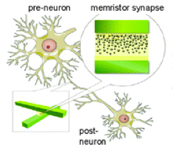
We now know that neuro-plasticity describes the ability of human neuronal networks to selectively form stronger or weaker connections as examples of adaptive learning. Neurons are triggered by ionic transport across the synaptic cleft—with nominal spacing <10nm (figure)—and since a neuron’s function varies with an “action potential” that creates non-linear dependencies, a memristor may be the closest solid-state electronic device we have found that mimics the function of a neuron.

Perhaps dense arrays of memristors could be somehow wired together to learn from inputs so as to create artificial intelligence (AI). Researchers in the Lu Group at the University of Michigan have already shown that, “a hybrid system composed of CMOS neurons and memristor synapses can support important synaptic functions such as spike timing dependent plasticity.” Maybe a massive memristor array will eventually be part of a system that will pass the Turing Test, and we’ll be one step closer to meeting Marvin the Paranoid Android. –E.K.

Monday, April 5th, 2010

The 2010 SPIE Advanced Lithography conference is where we first get glimpses of the future of nano-scale patterning technology for manufacturing. Sometimes, many fuzzy blobs come into focus as a picture in a single moment, and Yan Borodovsky of Intel showed how to do 22nm node litho the day before SPIE officially started. At both Nikon Precision Corp.’s afternoon event, and again at KLA-Tencor’s event in the evening, he showed the tremendous advantages of forcing IC designs into stacks of one-dimensional (1D) patterns.

With optical lithography limited to 193nm illumination and 1.35 N.A. lens-stacks, there are now serious scaling limits in high-volume manufacturing (HVM) of ICs. No matter what source-mask optimization (SMO) tricks are used, the limit to the pitch that can be patterned in a single exposure using a resist with a monotonic relation between dose and development rate is 72nm. Extreme ultra-violet (EUV, at 13.5nm wavelength) lithography is not ready, electron-beam direct-write (EBDW) is too slow, and directed self-assembly (DSA) of molecules remains unproven for IC patterning.

IC standard cell designed with one-dimensional layouts (source: Tela Innovation)

IC standard cell designed with one-dimensional layouts (source: Tela Innovations)

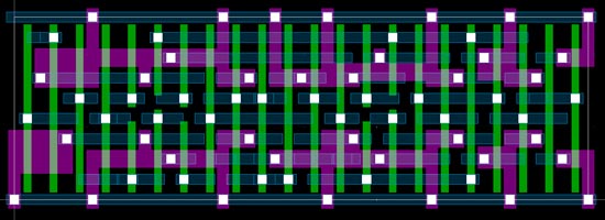
Consequently, it has become more and more expensive to make 2D patterns, and at some point we have to accept the design constraint of strict 1D layouts for logic. While IBM/GlobalFoundries claims to want to keep 2D layouts for logic, Intel began transforming its design intellectual property (IP) from 2D patterns into essentially 1D patterns years ago, and is currently in HVM using lines with a second “cut” mask for logic chips. Sidewall spacer pitch doubling is used for HVM Flash memory today. TSMC is working with Tela Innovations to promote the concept of highly regular layouts; Tela licenses standard cell IP (figure) as well as 2D-to-1D layout transformation services.

Chris Mack, gentleman scientist, provided a wonderful daily blog from SPIE this year, and his February 23 posting summarizes the recent clarity:

“I find it very interesting to see various players in the industry slowly getting behind this basic double-patterning strategy: Designs are restricted to essentially one-dimensional features of a single pitch on a grid. The first patterning step uses 193i with sidewall-spacer pitch doubling that can get the final pitch down to around 38 – 40 nm. A second patterning step then cuts the lines to make the final pattern. The resolution of the second patterning step determines the tip-to-tip spacing of the line patterns, but is a secondary (though important) influencer of packing density. What tool will do the cutting? Immersion with all the optical tricks? Multiple e-beams? EUV?”

To allow for routing connections in logic circuits, the transistors cannot be packed as closely as possible. Generally, compared to the line width, the space between lines is set three times greater. “It turns out that 1:3 is the sweet spot for gratings if you have a low-flare tool,” commented BetaSights’ M. David Levenson. “So long as you can keep the true pitch above 80nm or so, 193i will work for 1-D gratings with one exposure.”

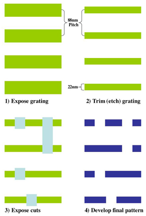
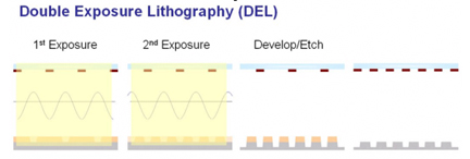
One exposure forms regular dense line arrays, followed by plasma etching to “trim” the linewidths, followed by the second “cut” exposure, to form the final pattern.

One exposure forms regular dense line arrays, followed by plasma etching to “trim” the linewidths, followed by the second “cut” exposure, to form the final pattern.

For 22nm logic transistor minimum gate dimensions, the first step is to create gratings of periodic and uniform lines and spaces at 88nm pitch. Then a traditional plasma etch tool “trims” a few nanometers from the sides of the lines to form the grating structures with 22nm lines and 66nm spaces. After exposure with the second “cut” mask, the pattern is transferred to the wafer (figure). This fab flow is what allows Intel to enjoy low defect levels and high yields in HVM. Though two patterning steps are needed, the costs are minimized since each step is easier and proper design can expand the overlay tolerance.

Periodic Structures is a new startup-launched with some US government funding-that is trying to create a new exposure tool designed exclusively to form (as per the company name) periodic gratings for the first exposure in this flow. Talking with BetaSights, co-founder Rudi Hendel explained that it’s overkill to use lenses capable of 2D patterning to form gratings, and that they have proven the concept of a significantly less expensive 1D imaging system.

Even with the most efficient “mix & match” exposure tool strategy, double-patterning flows are certainly complex. Former Intel lithography expert Alexander Starikov, current operating I&I Consulting, in a private conversation with BetaSights, wisely noted that all double-patterning schemes actually require three patterning steps for metal interconnect layers! This is because the edges of regular arrays in one IP block generally have to connect with another array or bond pads and somehow non-regular patterns must be formed.

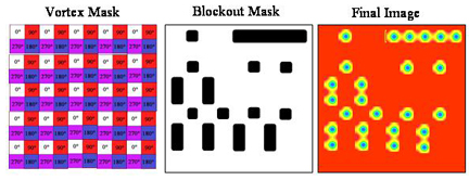
Levenson has identified and long promoted another lithography approach that is conceptually similar to line-cut double-patterning: “Vortex-blanking” double-patterning. Used to form contact patterns, a regular “Vortex Array” mask creates minimally sized dense arrays in a single exposure, to be followed with a second blanking mask to create the final sparse contact pattern for logic (figure). In this method, the phase-shift mask (PSM) structures create the finest spacings possible in a single exposure of a negative resist, and then the block-out mask exposes the ones that you don’t want to print.

Two exposures with Vortex array and blockout (“trim”) mask equalizes CDs across pitch (source: M. David Levenson)

Two exposures with Vortex array and blockout (“trim”) mask equalizes CDs across pitch (source: M. David Levenson)

The limit of HVM litho so far has probably been seen in research for the hard-disk-drive (HDD) industry. To get to the smallest possible patterned bit media (PBM), researchers first use EBDW to form sparse posts, followed by DSA of co-polymers to form dense arrays, followed by pattern transfer to form nano-imprint-litho (NIL) master templates with the densest possible 1D structures. Of course, there are essentially no overlay issues with HDD media.

NIL hope for 2D

Perhaps the last best-hope for 22nm 2D patterns comes from NIL. In private conversation with BetaSights, Mark Melliar-Smith of Molecular Imprints Inc. said that his company’s NIL overlay has already been reduced below 20nm in mix and match applications with a 193nm immersion stepper. Data taken at SEMATECH indicates that overlay can be improved with frequent template cleaning or overfill-insensitive alignment marks. At 22nm, Melliar-Smith predicted his company’s jet and flash imprint lithography (J-FIL) technology will have the lowest CoO – neglecting mask cost.

Mask cost and lifetimes may not be a gating factor for the adoption of NIL in HVM of ICs. DNP has already produced 14nm line-space J-FIL masks, according to Naoya Hayashi of DNP. Masks with the 22nm patterns needed for NAND flash in 2013 can now be produced using a 50KV e-beam tool. The etch depth uniformity of 1.8nm is good enough already. However, Hayashi worries that there is no inspection tool for imprint templates, forcing vendors to rely on wafer inspection. Even a new Hermes MicroVision inspection tool will take 32 hours to inspect one field. DNP expects to begin production of replica templates by imprinting the master masks in 2012. Template repair has been proven to work at 32nm, Hayashi reports. -E.K.

Monday, March 22nd, 2010

The upcoming Spring Materials Research Society (MRS) Meeting in San Francisco will feature a separate “Nanocontact and Nanointerconnects Workshop” to explore the biggest secret about the smallest devices: for the near-term there’s nothing better than standard metal. The workshop will address both theoretical and experimental approaches to formation, carrier transport, and reliability, and so will also explore the long-term potential for novel materials and structures.

Whether it’s a quantum dot for memory, a self-assembled molecule for a switch, or a carbon-nanotube (CNT) sensor, it needs electrical connections for power and signals. As new materials with novel composition and geometry are explored, the underlying physics of contact/interconnect formation and carrier transport needs to be re-examined.

The scheduled speakers for the all-day event are as follows:

  • Stan Williams, HP Labs (plenary), Palo Alto, USA
  • Paul S. Ho, University of Texas, Austin, USA
  • Suzanne Mohney, Penn State University, USA
  • Francois Leonard, Sandia National Labs, USA
  • Juan Jose Palacios, Universidad de Alicante, Spain
  • Richard Martel, University of Montreal, Canada
  • Jon Pelz, Ohio State University, USA
  • Ingann Chen, National Cheng Kung University, Taiwan
  • Hanno H. Weitering, University of Tennessee/Oakridge National Lab, USA

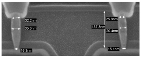
In the real world of high volume manufacturing (HVM) of nanoscale devices, the performance is typically gated by the interconnect. The speed of the switch is now generally faster than the time needed to get electrons to flow down the wire to the switch. The resolution of the sensor array is now limited by the shadows from the wires. Converting a signal between electrons and photons—using detectors and laser diodes—adds unacceptable delay. No one has found a room-temperature superconductor, and after decades of research there is not even a hint that one could exist. In all, there’s nothing better than a 15nm copper contact (see figure).

SEM cross section of 15-16 nm Cu contacts post-anneal. There is no Cu diffusion through the Ru to the silicide, and no void formation. (source: IBM)

SEM cross section of 15-16 nm Cu contacts post-anneal. There is no Cu diffusion through the Ru to the silicide, and no void formation. (source: IBM)

Just over two years ago at IEDM 2007 in Washington, D.C., an evening panel discussed “Looking beyond silicon – a pipe dream or the inevitable next step?” While most of the discussion had focused upon so-called “More than Moore” devices (beyond silicon-based CMOS), one of the final conclusions was that interconnects appear to be our real limitation. “There is no new switch in sight,” said Wilfried Haensch, IBM senior research manager. “All candidates are either non-manufacturable or they can not be wired up.”

So, any proposed new nanodevice must outperform CMOS, and for the near-term must rely upon the same connections as available to standard silicon CMOS. As the International Technology Roadmap for Semiconductors (ITRS) 2009 edition’s Emerging Research Devices (ERD) section mentions on page 23, “An accelerator that is offered as a CMOS replacement should offer a performance improvement relative to its CMOS implementation of an order of magnitude.” To justify the R&D costs and integration risks, any new conductor technology would likewise probably have to provide an order of magnitude improvement in performance.

Christopher Case, ITRS Interconnect TWIG Chair (currently with Solid State Solutions), writes in the January 2010 issue of Future Fab (special ITRS issue) that Cu is expected to be our interconnect for at least the next 15 years. For any interconnect to complete with nanoscale copper contacts, Case reminds us that, “the goal is propagating terabits/second at femtojoules/bit.” He provides an excellent overview of the inherent challenges in trying to improve upon copper contacts.

As Case reminds us, from first principles of materials it seems that the only way to improve upon today’s copper contacts is to eliminate the internal grain boundaries that induce electron scattering. We can grow CNTs or single-crystal metal fibers from nanoscale catalyst dots, but we’re still only at the proof-of-concept stage. We’ve discovered graphene, but we’re still just beginning to learn about what we have yet to prove. If you attend the MRS Nanocontacts and Nanointerconnects Workshop in two weeks, you’ll probably learn the lower size limits of what we can build today and most of tomorrow.—E.K.

Monday, March 15th, 2010

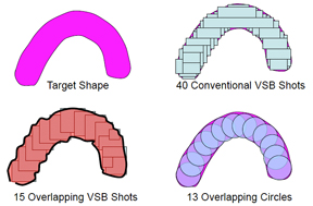
Another back-to-the-future possibility for next-generation lithography (NGL) is direct write e-beam (DWEB), revitalized with multibeam clusters, curvilinear mask writing, and character projection (CP). The E-beam Initiative used the recent SPIE gathering to announce that it had added six new member companies, including GlobalFoundries and Samsung. Aki Fujimura, CEO of D2S and Managing Director of the E-Beam Initiative, announced design for e-beam (DFEB) mask technology from D2S which enables fracturing into circles as well as rectangles, and allows overlapping shapes to create curvilinear features with far fewer e-beam shots.

Since masks are becoming more curvilinear, shot count is exploding for today’s vector systems. Cell projection as promoted by the E-beam Initiative thus appears to be a newly affordable solution. Since contacts always appear round on the wafer, Fujimura advocates a standard circular aperture for printing contact patterns on masks in one shot, rather than doing OPC with several. The wiggly assist features typically needed for inverse lithography can also be more easily printed with circular or arc-shaped beams, according to Fujimura.

Much of the DFEB value—as presented by Fujimura—lies in overlapping e-beam shots to create better images in less time (see figure). Using conventional, non-overlapping, rectangular VSB shots to achieve this shape, as shown in the upper right, requires 40 VSB shots. By using overlapping rectangular shapes, the shot-count can be improved to 15. However, by using overlapping circular shots, the shot-count is further reduced to just 13 – an almost 70% reduction in shot count over the conventional approach using nonoverlapping rectangles.

Franklin Kalk of Toppan Photomasks highlighted the need to reduce shot count to speed mask production. Today, he said, the capital expenditure for a 22nm mask line is >$100 million, but the output would be one mask/day, without some innovation. It needs to speed up by at least a factor of two to keep 193nm immersion lithography viable for the next 5-6 years.

Mapper Lithography continues to be the most plausable on-wafer maskless technology, but its progress may be too slow to intercept the 22nm node, and so along with other European programs, it may be re-focusing on the 16nm and 11nm nodes. Still the company proudly announced that a “pre-alpha” demo tool installed at TSMC Fab 12 in Taiwan continues to do R&D work on advanced nodes.

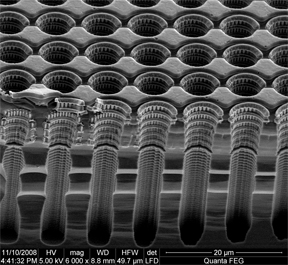
To increase throughput to the required 10 wph level with available technology, Mapper has re-engineered the company’s system to employ a dispenser cathode, at 0.3nA per beam and 7×7 beam parallelism to increase the total dose on wafer to the required 13nA. That results in a considerable increase in complexity as now there are 637,000 apertures, a condenser lens and a beam cross-over in the Mapper system. Still, technology development continues with 7X7 blanker arrays fabricated at 8mm pitch in CMOS using 180nm node fab technology at TSMC (see figure).

Yan Borodovsky of Intel confided to everyone throughout the week that his ideal litho system for Intel-type layouts would be line and cut lithography, with the lines printed using sidewall double (or quadruple) patterning and the cuts probably done using a high throughput EBDW system.

At the KLA-Tencor lithography users forum prior to SPIE, Borodovsky disclosed Intel’s “rule of thumb” target for the economics of any next-generation lithography approach: US$0.5M in tool price for each wafer-per-hour (wph) throughput specified. Thus, if the tool cost is expected to be $50M then for desired layers the tool must provide 100 wph. With 5KeV Mapper EBDW, to hold to 2nm overlay tollerance the best throughput is probably 1 wph, while loosening the spec to 4nm allows for 10 wph. If the percent exposure is only ~5% for trim, instead of the nominal 50% for most full-field mask layers today, then the relatively relaxed 4nm spec could indeed provide 100 wph.

Borodovsky also shared modeling results for the scattering of electrons into resist to establish reasonable expectations for image blur. Over the 5-50 KeV acceleration range typical for systems considered for EBDW, minimal blur was seen at expected resist thicknesses.

Borodovsky showed data taken by researchers at Technion Israel Institute of Technology in high-k metal-gate (HKMG) transistor damage from 30 keV EBDW, and saw damage due to breaking SiO2 bonds (typically 3-6 KeV bond energy), and slight reduction in dielectric constant (11.7 to 11.5k) resulting in threshold voltage shifts. However, a simple 300°C anneal for 2 minutes in air restores the k to 11.7 by healing the broken bonds. While the ability to heal the HKMG damage is enouraging, we may be safer using some manner of an ultra-thin “charge distribution layer” (CDL), to be integrated with the ARC layer, to shunt electrons away from underlying transistors during interconnect processing.

EBDW for HVM in 2015 still has capability gaps according to Borodovsky: production readiness, wafer defects, throughput, data corruption, and channel-to-channel skew (with thousands of channels). Nonetheless, EUV seems even less capable today and has added mask costs, and some manner of NGL technology will be needed to pattern sparse layouts. Therefore, maskless EBDW may finally reach the mainstream of IC production in the next few years.—M.D.L. and E.K.

Monday, March 8th, 2010

This year’s plenary sessions of the SPIE Advanced Lithography Symposium exposed the complexities of patterning ICs in high-volume manufacturing (HVM) at the 22nm node and beyond. Steppers using 193nm ArF immersion (193i) will be extended using double-patterning (DP) schemes, since the extreme-ultra-violet litho (EUVL) infrastructure is again delayed. R&D to support DP integration has led to the creation of a “Texas two-tone” photoresist requiring only a single developer.

Kazuo Ushida, President of Nikon Precision Equipment (source: SPIE)

Kazuo Ushida, President of Nikon Precision Equipment (source: SPIE)

The technical sessions began with a prediction of better times ahead by plenary speaker Kazuo Ushida, President of Nikon Precision Equipment. Ushida noted that the wafer fab equipment industry cleared only $12B in revenue in the terrible year of 2009, but that predictions were for $20B in 2010 with recovery to the 2007 level of $25B by 2011. As usual, the growth in semiconductor revenue will be driven by a Moore’s Law increase in functionality, but achieving that–and particularly the lithography part of achieving it–had become especially difficult. Ushida outlined various possibilities for the future, beginning with a continuation of today’s trend for double patterning using 193nm immersion steppers, some new technology (like EUVL), and stopping the circuit shrink altogether.

Ushida conceded that the EUVL infrastructure was developing too slowly for insertion at the 22nm node. Useable masks might not be available until after 2014 even if someone came up with the $130M needed to develop a mask inspection tool and the defect density of EUV masks and substrates improved 100 fold. To be profitable, a new lithography has to be good for two nodes when introduced, so a tool developed for 16nm node insertion must be useable at 11nm as well. The most likely design for a high volume production EUVL tool then involves a larger numerical aperture (NA) and the compatibility with resolution enhancement technologies (RETs) like dipole illumination. Those RETs, in turn, imply more restricted design rules, such as are being implemented for flash memory today. The higher NA means more mirrors, and an even more powerful source to attain required throughput.

Double patterning, especially using self-aligned spacers to form grating-like-designs, has a natural way forward: the pitch doubled spacers can be used as mandrels for another spacer deposition, perhaps ad inifinitum! The problem is with the cut mask, which defines line ends. Already the cut holes need to be shrunk chemically, but much fancier RETs are coming. Ushida pointed out that extending 193nm lithography in that way would need cost reducing innovations such as tool and mask re-use to remain viable.

The second speaker, Eric Chen of Silverlake Partners, pointed out that future growth was going to be different from the past. In particular, the developed economies have assumed so much debt that they will have to deleverage rather than consume in the coming “reset economy.” Growth, he predicted, would result from increased consumption in emerging markets like China. Developing and manufacturing products for those markets was going to be disruptive for today’s business models. Fast time to market, niche targeting, and low margins would drive the R&D environment. New leaders like Huawei and ZTE would emerge to compete with western technology companies.

Sam Sivakumar of Intel (source: SPIE)

Sam Sivakumar of Intel (source: SPIE)

Sam Sivakumar of Intel focused on the meaning of these economic changes for future lithography. He deconstructed semiconductor lithography as a play in four acts. In Act1, lithography delivered design intent to the wafer automatically. In Act2, litho manipulations like OPC were sufficient to insure that design intent was realized. However, in today’s Act3, only certain geometries can be printed and thus the designs must be restricted to litho-friendly one-dimensional layouts, etc. In the coming denouement, computational lithography will be required up front to co-optimize proposed layouts, illumination, OPC decoration, and processing.

Thus, Sivakumar warned, the architects of litho design and process must collaborate for success from now on. Further, mask making has become an integral part of lithography planning and cannot be treated as a commodity service. The single biggest future problem would be containing the cost of patterning, he averred.

Complexity increases cost while area scaling reduces it. Sivakumar advocated reducing the number of geometrically complex layers to increase value. He also worried about the cost of EUVL. He warned that EUV masks had to be assuredly defect free as used in the stepper because look-ahead wafers would economically insupportable in any plausible EUVL production scenario. That made EUV mask inspection essential for the success of EUVL and an opportunity for tool vendors to pursue.

Resist and Processing

The keynote talks in the resist symposium were not all about resist. Rather, John Sturtevant of Mentor Graphics began by reviewing the evolution of computational lithography and the models needed to predict resist patterns on the wafer. He emphasized that the algorithms used to apply OPC decoration to a full chip design would always be different from the ones used on TCAD clips for optimization and parameterization. Exotic resist behavior cannot be easily accommodated in models and he wished it could be avoided. At 32nm, a one layer OPC run takes 24 hours on a 400 CPU system, and there are 35 layers now requiring OPC. A modeling accuracy of 1nm is achievable today, he claimed.

Ralph Dammel of AZ Electronic Materials speculated on the chemistries that might be needed for future production. He suggested that planar processing would continue to progress, with graphene eventually replacing silicon as the active layer. The immediate challenge was to do double patterning cost-effectively, though. He outlined several schemes being pursued to avoid an intermediate etch into a hardmask layer, but requiring 6 to 15 steps in the litho cell. None had yet been proved manufacturable, in Dammel’s opinion. Further ahead, Dammel predicted that efforts to develop EUVL resist would break out of the “triangle of death” defined by resolution, sensitive and LER tradeoffs to yield a useful 16nm resist by 2014 or 2015. Before that, he predicted an industry bifurcation where some segments would abandon shrink altogether when optical lithography finally runs out of steam around the 22nm node.

Subsequent speakers described exotic resist systems that might be used in double patterning lithography. Shinji Tarutani of Fujifilm Corp described negative tone resists for 193nm exposure of the sort which could be used for copper interconnect trenches or contacts in a double exposure double etch scheme. Unfortunately the FujiFilm materials required organic solvent development and showed two orders of magnitude less contrast than common positive resists. Still, one had been used at IMEC to pattern 45nm contact holes on a 90nm pitch with 3-4nm CDU.

Double exposure in a single resist cannot beat the Fourier optics (k1=0.25) pitch limit if the resist responds linearly, but what if the resist were non-linear in some useful way? Robert Bristol and a team from Lawrence Berkeley laboratories used double exposure experiments to seek out non-linear (non-reciprocal) behavior in potential resist materials. They found a system that produced a photo-base generator when exposed to 193nm light and subsequently flood exposed at 365nm. A second 193nm exposure released the base, allowing development of a pitch less than could be patterned in either 193nm exposure separately. They demonstrated a k1~0.125 but a pitch of 900nm.

Texas Two-Tone

Xinyu Gu and a team from the Willson lab at the University of Texas, Columbia University, and Intel showed a true two-tone aqueous TMAH developed resist for 193nm exposure. A two-tone resist works like a positive resist at low dose, so unexposed material remains on the wafer, but at high exposure it becomes negative-working, so that heavily exposed regions also remain (see figure). Only at intermediate dose levels does such a resist dissolve in developer, which halves the pitch of a properly exposed pattern.

Gu explained that the Texas Two-Tone resist functioned because it contained a low concentration of photo acid generator and a higher concentration of a lower-efficiency NO2–releasing photobase generator in a conventional CA polymer resin. At low dose, only the PAG exposure mattered and the CA resist was positive. However, once the PAG had all been consumed, increasing dose continued to produce more and more base, ultimately consuming the acid and stopping deprotection and development. A 56nm half-pitch mask resulted in a 26nm line-and-space resist pattern when developed in TMAH.

The Texas Two-Tone resist was termed the most important development in the last 10 years in a comment by Will Conley of Freescale Semiconductor, a recognized industry expert. It does seem more likely to be used in production than resists that require two developers to print both tones: one aqueous and one an organic solvent.

Charles Pieczulewski of Sokudo, a track vendor, explained that tracks were being built for two developers and even two resists for double patterning. Why two developers now? Well it turns out that there is something new in that area as well: 0.26N TBAH, an aqueous base developer that does not diffuse into resin as much as TMAH and thus improves contrast and wall slope while reducing pattern collapse! Adding a solvent developer is not a big step. –M.D.L.

Monday, March 1st, 2010

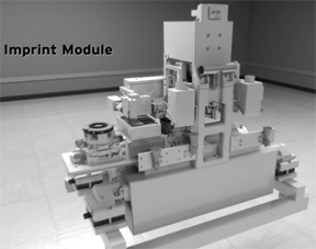
Molecular Imprints, Inc, announced their first nanopatterning tool designed for pilot and volume production of patterned hard disc drive (HDD) substrates at the SPIE Advanced Lithography Symposium in San Jose, CA February 22. The NuTera HD7000 uses Jet and Flash Imprint Lithography (J-FIL) technology to print over 300 double sided disks per hour up to 95mm diameter. The cost of patterned media lithography with the new tool is claimed to be less than $0.50 per disk, excluding the template cost.

One of the print heads in the Imprio HD2200 nanopatterning tool (source: Molecular Imprints).

With four print heads (see figure), the HD7000 has a footprint 40% smaller than the previous HD2200 tool. The new tool is also equipped for factory automation with interface flexibility to accommodate various cassette formats. Consumables are minimal because the enhanced IntelliJet drop patterning technology dispenses picoliter droplets of resist exactly where needed, with no waste.

Mark Melliar-Smith, CEO of Molecular Imprints revealed that the first two tools had passed Beta test in Austin and one had been shipped to an undisclosed hard disk drive manufacturer. This order brings the total systems sold to the HDD industry by Molecular Imprints to 13, as manufacturers focus on transitioning into the terabit era through their implementation of patterned media.

“Patterned media is essential to HDD manufacturers in realizing sustainable gains in areal density beyond the one terabit threshold,” stated Mark Melliar-Smith. “HDD manufacturers are currently leveraging the high-resolution patterning performance of our J-FIL technology in their patterned media development programs. As the first nanopatterning solution capable of pilot- and volume-production applications, the NuTera HD7000 serves as a critical vehicle to the ultimate goal of achieving patterned media volume production.”

In a separate interview with BetaSights, Melliar-Smith also described the progress in replicating templates using their Perfecta TR1100 tool. Since master masks for hard disk drives take weeks to write using Gaussian beam electron lithography with rotating stages, perfect and damage free replication of those masters is essential to an imprint lithography paradigm. Two TR1100 have been shipped, one to Hoya, a mask maker and one to an HDD manufacturer. These tools are being used to replicate templates on 6” round substrates at speeds of up to 10 per hour. The replicated templates, in turn, are used to pattern the final discs using the J-FIL process.

Low cost patterned media is now seen as essential to progress in HDD density, which has grown faster than Moore’s Law for decades. However, now there are fundamental stability issues for the small magnetic domains on today’s flat disks. The solutions contemplated begin with discrete tracks – essentially lines and spaces printed concentrically around the disk with pitch below 50nm – and progress into bit patterning with ~20nm dots arrayed in tracks. Even now, complex servo patterns along with the tracks, making the challenge more similar to that in the semiconductor industry than one might expect, according to Melliar-Smith. Thus the NuTera HD7000 enjoys some synergy with other Molecular Imprint programs.

IC plans (UPDATE 100308)

With the realities of line edge roughness and Fourier optics impacting the design and yield of both optical and EUV lithography, where can the IC fab industry go for arbitrary patterns printed smoothly? According to Melliar-Smith, it will be his company’s J-FIL system! Overlay has already been reduced below 20nm in mix and match applications with a 193nm immersion stepper. Data taken at SEMATECH indicates that overlay can be improved with frequent template cleaning or overfill-insensitive alignment marks. At 22nm, Mellair-Smith predicted J-FIL will have the lowest CoO – neglecting mask cost.

Mask cost and lifetimes may not be a gating factor. DNP has already produced 14nm line-space J-FIL masks, according to Naoya Hayashi of DNP. Masks with the 22nm patterns needed for NAND flash in 2013 can now be produced using a 50KV e-beam tool. The etch depth uniformity of 1.8nm is good enough already. However, Hayashi worries that there is no inspection tool for imprint templates, forcing vendors to rely on wafer inspection. Even a new Hermes MicroVision inspection tool will take 32 hours to inspect one field. DNP expects to begin production of replica templates by imprinting the master masks in 2012. Template repair has been proven to work at 32nm, Hayashi reports. –M.D.L.

Saturday, February 20th, 2010

The SPIE’s 7th Frits Zernike Award for Advances in Optical Microlithography goes to M. David Levenson, BetaSights Litho & DFM Editor, in recognition of one of the most important developments in lithography resolution enhancement of the last twenty years, the phase shifting mask (PSM). About 30 years ago at the IBM San Jose Lab, Levenson conceived the alternating PSM (alt-PSM).

UPDATE: In presentation #7641-27 of SPIE’s DFM session, Richard Schenker said Intel has now made over ONE BILLION chips using alt-PSM, starting at the 180nm node (HVM about ten years ago), for gate and for contact layers (the latter with sub-resolution assist features). –M.D.L., February 26th
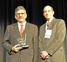
M. David Levenson receives the 7th SPIE Zernike Award from Chris Progler (source: Amy Nelson, SPIE)

M. David Levenson receives the 7th SPIE Zernike Award from Chris Progler (source: Amy Nelson, SPIE)

Dr. Marc David Levenson graduated from MIT in 1967, received his PhD degree from Stanford University in 1972, and post-doc’d at Harvard. He later became an Associate Professor of Physics and Electrical Engineering at USC in Los Angeles before joining the IBM San Jose Research Laboratory in 1979, where he worked on laser applications in science and technology, including quantum optics. Best known in science for his book “Introduction to Nonlinear Laser Spectroscopy,” in technology he is famous for originating the PSM. During the retrenchment at IBM in 1993, he left to help form Focused Research (a div. of New Focus, Inc.). Later, he held visiting positions at JILA (U. of Colorado at Boulder) and Rice U. in Houston, Texas. Until one year ago he was Editor-in-Chief of Microlithography World Magazine and he remains proprietor of M.D. Levenson Consulting as well as Litho and DFM Editor at BetaSights.net. He is a Fellow of IEEE, OSA, and APS, and a member of SPIE and National Academy of Engineering.

BetaSights founder and editor Ed Korczynski posed the following questions about physics, lithography, and what it’s like to try to lead the world through both metaphorical and literal darkness.

When did you first decide to become a physicist, and was there a particular teacher/mentor who sparked your interest?

I was probably always interested in science, but began focusing on physics in junior high. Partly it was the influence of Scientific American, which my father subscribed to, and partly it was the availability of cool cheap stuff from Edmund Scientific. I remember Sputnik and hearing its beep on a short-wave radio…that changed things. There also was the fact that my chemistry set experiments tended to produce disastrous results!

I don’t recall any outstanding teachers in West Virginia in my early years. The junior high science teacher decided we needed to do better on the Achievement Test, so he gave us the answers. I realized that, if I was going to learn anything, I would have to teach myself.

The laser fascinated me from the beginning and I remember going to an IRE meeting in Pittsburgh with my father, where some lecturer spoke about the earliest discoveries. When I got to MIT, there was an open-cavity HeNe laser in the freshman lab (and a Spectra Physics black-box laser to line it up). I learned to make it work and fiddled with the modes and diffraction patterns.

Unfortunately, when I needed a job as an undergraduate, the laser group had nothing. So, I got a job at the Laboratory for Nuclear Science and built equipment for particle physics experiments at the Cambridge Electron Accelerator. The CEA had blown up just before my job was to start and we had to do a lot of rebuilding before we could run anything. Still, it was a wonderful period. I did my senior dissertation in particle physics and had access to more resources as an undergraduate at LNS in the mid-‘60s than I ever had again!

Had you been working on phase-shift phenomena in general while you were a tenured professor at USC, and was that why IBM Almaden Research recruited you?

I was working there on multiphoton laser spectroscopy and four wave mixing, not phase-shift. I lost a series of academic cat fights and began looking around when I realized that lots of people had lifetime tenure at institutions like San Quentin, but would give it up for a decent opportunity.

There were rumors of two good opportunities for a laser spectroscopist, which turned into offers: one at NIST in Gaithersburg and one at IBM in San Jose. I had been a summer student at IBM and my wife had connections at SRI and we both loved the weather here, so I chose IBM. In retrospect, it was a mistake. The project was in data storage, the photochemical hole burning memory. I thought I knew something useful about that technology, but it turned out that what I needed to know was to keep my mouth shut!

When you were started the R&D, did you know of anyone else working on phase-shift approaches to microlithography?

I didn’t know of anyone working on phase-shift at the time. However, it has turned out that Masato Shibuya at Nikon was thinking about the same things at the same time. He was in pure stealth-mode, though! I later found out that he had visited Fairchild just down the road from IBM after I had published the first paper, and was asked about the idea, but said nothing!

Prof. Hank Smith and his students at MIT had also thought about phase shift in the context of X-ray proximity but their idea was different from mine and more closely related to attenuated-PSM, which was ultimately proposed by Burn Lin.

There had been different applications of phase-shifting plates in holographic data storage that were turned up by the patent attorneys later. I didn’t know about any of them. Today, they use gigantic plates like that to homogenize the laser beams at the National Ignition Facility in Livermore!

What has surprised you in the timing or manner of PSM use in industry since the invention?
I am amazed that it took over 25 years for the alt-PSM to be adopted here. There just was so much resistance, and not all of it from IBM management! Hitachi put an Alternating PSM on the cover of their annual report in 1989 and no one in the U.S. did anything. Even now, there are very few alt-PSMs being built in the world. My former company, IBM, never did succeed in using it to produce high-yielding chips, although they began making thin film heads with alt-PSMs soon after I left. There never was adequate R&D support for alt-PSMs and now it is too late.

On the other hand, the attenuating-PSM was adopted rather quickly, even before the materials problems were really addressed seriously. I had been told by the “experts” at IBM that depositing and etching uniform films with specified attenuation and phase-shift was essentially impossible. That may actually have been true, but the technology worked anyway! Now, of course, the neglect is showing itself as polarization issues come to the fore.

You continue to consult on optical microlithography technology development; can you tell us (in general) about some areas of interesting work you’ve done in the last 10 years?

The 21st century hasn’t been so great so far! Lately, I have actually been trying to go back to laser spectroscopy and quantum optics. However, I did get to collaborate with some wonderful people at DNP, Canon, Applied Materials and KLA-Tencor on phase-shift related ideas, most of which were not applied.
There was the Vortex mask that would have printed the finest possible pattern of vias, if negative resist were available. It was at KrF wavelength, but not really at ArF, even now. If you print those tiny dark spots in positive ArF resists, you get little posts, which all fall down! I think IMEC is still working on that using our mask….

We also did double patterning using the LELE and LPLE schemes at the Mayden Center in 2003 using alt-PSMs. We broke the k1=0.25 barrier using available materials, but at KrF wavelength, which meant the line/space half pitch was 70nm. Of course, everyone was on to ArF by then and the double patterning technology wasn’t yet ready at 193nm. It still isn’t!

Do you have any official opinions about the likely usefulness of EUV lithography for commercial IC fabs?

We really have to hope that EUVL will be successful, but I personally have grave doubts. To me it looks like a re-run of the 1X synchrotron X-ray debacle, where the R&D managed to stay just behind the leading edge of established technologies for several Moore’s Law generations. That enabled nice long R&D careers for many X-ray promoters, but harmed the industry as a whole.

EUVL is very, very hard technically and the business case has never been worked out for the whole food chain. Key bits of the infrastructure lag badly due to underinvestment and other parts are prohibitively expensive. My guess is that EUVL will be used for some classes of chips, but not widely and not profitably. The roll-out will be slow and the throughput per dollar will be low. Innovators will be able to side-step the limitations of other technologies before EUVL gets its act together. For example, Intel and Micron are making 25nm half-pitch NAND flash memories today. I think it is being done with sidewall double patterning, which is way cheaper than EUVL. If they can use that technology to make logic or DRAM, it is game over!

You’ve famously summarized one the fundamental principles of PSM as “there is no wavelength of darkness;” could you elaborate upon this principle for those of us who do not engineer with photons?

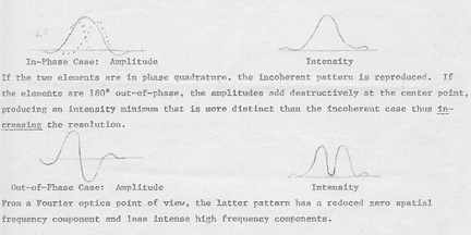
Everyone has heard of the “wavelength of light” and most engineers know that it sets a fundamental limit for the resolution of optical instruments, but the usual Rayleigh Criterion only applies to bright features. Criteria based on Fourier optics apply to gratings of bright and dark, so you hear about “pitch” and “half-pitch.” However, the size of the individual dark features between the bright ones is not set by the wavelength. Rather it depends on the criterion you set for the transition between dark and light (see figure from original 1980 patent application). Destructive interference in an image can make a line or spot of zero light intensity, but it has zero width. It you set the criterion for the edge of the dark line to be 10% or 20% or 50% of the maximum intensity, you get different widths. By the way, that was known to Lord Rayleigh. In practice, that means that overexposing photoresist can make very narrow lines.
When you first conceived that “there is no wavelength of darkness,” did it come as a pure conceptual abstraction or did you somehow visualize spatial/temporal phenomena?

Actually it was just a rhetorical flourish, based the need to get people thinking differently. By then we had done some dose-focus experiments and saw really extraordinarily narrow resist features, which unfortunately had all fallen over! I had calculated the minimum half pitch possible, which corresponds to a k1 factor of 0.25 – less than half the Rayleigh resolution. However, the dark lines were much narrower than that “half pitch!” The bright lines were wider.

Now, in practice, the width of the dark line is set by the stray light in the image – the so called “flare” which degrades CD control. Good lenses have low “flare” and a dark-field alt-PSM layout (as used by Numerical Technologies (bought by Synopsys) minimizes flare. So the way to reduce the dark CD is not to go to shorter wavelength but to better lens quality and design. Interestingly, the microscopists have developed a means of combating the effect of flare using 2 wavelengths of light, one that excites and one that de-excites molecules. They get 28nm images with visible light! Can we do that?

What is your favorite sub-atomic “thingie” (i.e., wave/particle/phenomenon), and what’s it feel like to explore the extreme limits of empiric knowledge?

My favorite thingie right now is back action evading measurement or quantum nondemolition measurement (QND). Those methods allow you to measure the very vacuum fluctuations and predict quantum results! It may not be as cool as teleportation or Bose-Einstein condensates, but it is a bit easier!

Scientific research is really hard at the frontier. You are at the limits of your own knowledge, everyone else’s knowledge (whether they admit it or not) and available technology. The theory and equipment generally doesn’t work and has to be fixed. When you solve one problem, you generally uncover two more, and that goes on and on. To layer politics and funding concerns on top of that as well as the need to keep predatory bosses at bay, well that just makes it too hard to endure forever.

But eventually if you are persistent and lucky, the last problem gets solved and it all works. That feels gratifying personally, but then you have to tell someone. If what you have done illustrates an important issue or seems useful in technology, it is very disappointing to see your result relegated to obscurity. It is even worse to be denied the resources to do anything else because you have already had a “success.” I am glad that I did manage to publish most of the work, but generally someone else published the same general thing at about the same time! A lot of it has now been independently re-discovered 20 and 30 years later.

So, recognition like this Frits Zernike award feels very gratifying!

Do you find Walborn’s 2002 “quantum erasure” experiment to provide conclusive evidence in support of Bell’s Theorem, why, and what are the ramifications for what we (and Einstein) like to call “reality”?

Alain Aspect authoritatively disproved local objective realism 20+ years ago. I have some quibbles with the quantum erasure and wechtel weg experiments, but they illustrate a valid point: quantum mechanics is about information that you have (or should have) about a system and nothing more – certainly not “reality.” Our universe has in it nonmaterial correlations that can appear to violate all reason. Sorry, but that is the way it is!

The nonlocal correlations seen in the Bell’s inequality demonstrations emerge only from non-local experiments. If all you have is the local information from a photon detector at your location, you get a meaningless random stream of polarization data. So does your collaborator at the other side of the universe. However, if you get together later and compare notes, you find the photon polarizations at the two detectors are more closely correlated with one another than they can be to any common source. Those are the EPR-Bell correlations. However, that is a non-local experiment and it should not be surprising that a non-local property emerges. Entanglement gets stranger with 3 particles. Check out the Greenberger-Horne-Zeilinger (GHZ) experiments!

Personally, I regard it as a bug in the operating system of the universe!

-E.K. and M.D.L.