Thursday, April 30th, 2009
Human intellectual development has eclipsed emotional development, with the resulting problem of clever people lacking morals. In government, industry, and academia there are endless examples of this problem, which is now threatening the economy due to corruption, and the very biosphere of the earth due to pollution. It is heartening that MIT (that trained most of the “Quants” who created the algorithms that floated the financial scams behind the current “global financial crisis”) today officially opens The Dalai Lama Center for Ethics and Transformative Values, with a talk by the XIVth Dalai Lama and a benefit concert by Philip Glass.
 The Center at MIT is dedicated to inquiry, to dialogue, and to the creation of programs that affect the ethical and humane dimensions of life. This nonpartisan center is a collaborative think tank focused on the development of interdisciplinary research and programs in various fields of knowledge from science and technology, to education and international relations. The Center is founded to honor the vision of the Dalai Lama and his call for a holistic education that includes the development of human and global ethics.
“We live in a time of profound change. Science and technology continue to expand our ability to understand and change life. Our impact on the environment has grown to the point that we are affecting the planet as a whole. Economies and societies can no longer be thought of separately, for they are intertwined in a global community. Our actions as individuals and as societies affect not just ourselves but our global neighbors. Now more than ever it is imperative that we contemplate and understand our relationship to and the impact of our actions on each other as individuals, as countries, and as inhabitants of our planet,” said Tenzin Gyatso, the XIVth Dalai Lama.
Individual decisions affect the economy and the environment, and regardless of your belief-system there are common values (and “secular ethics”) upon which we can base a functional system of ethics. This month, The Dalai Lama Center for Ethics and Transformative Values at MIT will host its first public event: The Human Impact Conference. It will be an interdisciplinary forum exploring ethical responsibility in the context of a globalized economy and an environment that is vulnerable on a planetary scale. Empowered by technology and communications, the influence of human actions now reaches far beyond what traditional ethical systems have envisioned.
The conference brings together scholars, policy makers, and global leaders for a wide-ranging public dialogue that invites us to recast our understanding of the ethics of personal responsibility on a global scale and to weigh the long-term effects of choices we make today. The list of invited speakers for spring and fall 2009 include APJ Kalam, Samdhong Rinpoche, Rigoberta Menchu Tum, Wangari Mathaai, Howard Zinn, Jane Goodall, Martha Nussbaum, Betty Williams, Fr. Thomas Keating, Richard Davidson, and Daniel Goleman. -E.K.
Tags: ethics, PV, R&D
Posted in fab, PV, Uncategorized | Comments Off on MIT opens Dalai Lama center for ethics
Wednesday, April 29th, 2009
Thermal management of advanced ICs remains challenging, with models often failing to predict the heat flow through multiple films and interfaces. Advanced Thermal Solutions (ATS) of Norwood, Massachusetts (US) will provide a half-day of free, no-obligation use of its unique Thermal Characterization Laboratory to engineers who need to perform thermal testing of their heat sinks, fans and fan trays, PCBs, blades, enclosures, or complete systems. Experienced engineers and board and system designers can perform the tests themselves, or consult with an ATS thermal engineer at no cost during their 4 hours of laboratory time.
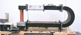
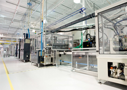
 ATS’ Thermal Characterization Lab features open- and closed-loop wind tunnels for ambient and elevated temperature testing (see figure). All wind tunnels are PC-driven controls and provide automated data collection. The lab also offers a full array of the company’s sensor systems and thermocouples, which can be used to characterize electronic products under variable airflow and temperature conditions.
The lab includes a JEDEC-approved component thermal testing facility for conducting various device-level tests. There are also complete liquid crystal and IR thermography systems for non-invasive temperature mapping (0.1 degree C temperature, and one micron spatial resolutions), and a liquid cooling facility for the complete testing and characterization of cold plates.
“Most of today’s electronics have thermal situations that can turn into big problems if left alone. The easiest, lowest cost way to manage this is to conduct an accurate thermal characterization of the problems at hand,” said Kaveh Azar, Ph.D., president and CEO of Advanced Thermal Solutions, Inc. “If you have the right facility and associated know-how, you can often complete your tests in a half-day, then you can readily assess what is the best thermal solution for your application.”
The company also supplies complete thermal and mechanical packaging solutions from analysis and testing to final production, along with thermal design consulting services and training. All testing and results reporting are completely confidential. Certain restrictions and limits on customer products may apply, e.g. overall size. Consultation prior to use of the lab is not charged or considered part of the free time offer. ATS thermal test engineers will also advise lab patrons how to optimize their free testing period prior to arriving. –E.K.
Tags: characterization, FPD, IC, MEMS, Service, test, thermal
Posted in fab, IC, MEMS, Product, PV, Service | Comments Off on Free thermal characterization lab time
Thursday, April 23rd, 2009
Silicon Valley has certainly not been immune to the current economic conditions, with many companies announcing multiple rounds of layoffs and moving operations overseas. Yet for many it is still considered “the heart” of the high-tech industry. At today’s well-attended Silicon Valley Lunch Forum, organized by the Sales and Marketing Council of SEMI, three speakers addressed the question of the future of Silicon Valley. Traditional silicon IC design and pilot production work, innovative printed ICs, and photovoltaics fabs are all part of the future.

All printed silicon TFT (source: Kovio)
“It is not the product, or the pricing or the support that has been key to the development of the Valley, but the networking opportunities,” declared Art Zafiropoulo, chairman and CEO of lithography tool maker Ultratech Stepper. In his view, the key challenge to the continued success of Silicon Valley is relatively high tax rates and cumbersome tax regulations. As a result, Zafiropoulo sees a future for Silicon Valley that will still be a high tech center in the areas of design, software and management but will no longer be a center of manufacturing. In fact, “the equipment industry will literally disappear in Silicon Valley and eventually in the United States,” Zafiropoulo predicted.
But the other two speakers see a slightly different scenario. Richard Young, vice president of operations for Kovio, a developer of printed silicon electronics, talked about his own company’s commitment to Silicon Valley. With a 22k square foot clean room in Milpitas, “Kovio has every intention of keeping manufacturing here in the valley and will be ramping production this year,” reported Young. While about 90% of all printed semiconductors are based on organic chemistries, Kovio has developed a 100% inorganic silicon printed transistor and was the first company to demonstrate an all-printed transistor as well as the world’s first silicon ink (see figure). According to Young, the printed silicon industry has the potential to one day be as big as the silicon industry is today.
Printed silicon electronics would fall under the category of “non-Moore’s Law products” as outlined by the final speaker, Dave Bergeron, chief technology officer of SVTC, speaking on emerging technologies in a changing market. Working with 200mm diameter wafers, SVTC has three manufacturing facilities, of which two are located in San Jose in the heart of Silicon Valley, a semiconductor fab and a solar fab that will be commission later this year. All facilities have a Class 10 Cleanroom. Most current SVTC customers are not trying to push Moore’s Law. Bergeron says their “sweet spot” is between 90 and 350nm structures. In Bergeron’s view, despite the current economic reality, “innovation will continue and especially in Silicon Valley.” He further explained, “there are a lot of people here in the valley with the background and knowledge to do this, and frankly it can’t get done anywhere else.” –E.S.
Tags: 200mm, CMOS, fab, IC, printed, PV, R&D, Si
Posted in fab, FPD, IC, MEMS, Product, PV, Service | Comments Off on Silicon Valley fab futures seen at SEMI lunch forum
Wednesday, April 22nd, 2009
Researchers at MIT have demonstrated deep subwavelength lithography using a photochromic contrast enhancing layer, as reported in SciencExpress April 9. A thin photochromic film on top of a conventional photoresist layer was exposed to two wavelengths of light with two distinct patterns. One wavelength exposed the photoresist while the other made the photochromic film opaque to that wavelength, without exposing the resist itself. These results demonstrate the feasibility of litho-litho-etch double-patterning (LLE-DP).

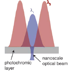
When illuminated with a node at Lambda2 coincident with a peak at Lambda1, an aperture is formed to reach the underlying photoresist. (source: MIT)
The molecules chosen to comprise the photochromic film adopt two isomeric forms that interconvert reversibly on respective absorption of light at ultraviolet (Lambda1) and visible (Lambda2) wavelengths. Sub-wavelength patterns result from applying both colors in an interference pattern that overlaps peaks at Lambda1 with nodes at Lambda2. Absorption at Lambda1 generates the isomer transparent at that wavelength, but regions exposed to Lambda2 revert to the initial isomer and continue to absorb at Lambda1, protecting the photoresist. Only at the Lambda2 nodes does a stable, transparent aperture form (see figure).
Photons at Lambda1 penetrate this aperture, forming a nanoscale writing beam that can pattern the underlying photoresist. The aperture size decreases as the ratio of the intensity at Lambda2 to that at Lambda1 increases. Because there is no wavelength of darkness to limit the width of this node, this absorbance modulation can confine light to spatial dimensions far smaller than the wavelength of light. The pitch, however, is limited by Lambda2. More on this in the BetaSights Newsletter. –M.D.L.
Tags: 22nm, 32nm, DP, IC, litho, LLE, mask
Posted in fab, IC, Material, Product | Comments Off on Deep sub-wavelength nanopatterning
Tuesday, April 21st, 2009
IMEC has successfully transferred memory variability aware modeling (MemoryVAM), the first EDA tool for statistical memory analysis, to Samsung Electronics. The tool predicts yield loss of embedded SRAMs caused by the process variations of deep-submicron IC technologies. This may be the first proven design-for-manufacturing (DFM) tool to provide statistical analysis across degrees of abstraction from the transistor up to the netlist level. The tool can reportedly avoid design respins by accurately estimating yield losses due to both static and dynamic process variations.

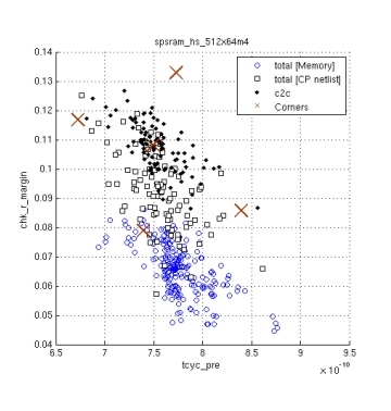
Typical outcome of MemoryVAM for embedded memory, showing preserved correlations for global and local variations of cycle time and read margin for both the CP netlist and the memory. The crosses show a comparison to corner-based simulation. (source: IMEC)
Process variability was in the past defined by corners: boundaries in parameter variation that accounted for process tolerances. However, statistical variations now produce static random phenomena as well as suceptibility to time-dependent variations in supply voltage, temperature, and interference. As can be seen, corners no longer properly bound the functional space (see figure). The world has been waiting for statistical EDA for many years; this may be the foundation of how SoC are designed for the next twenty years.
“This is especially interesting for embedded SRAMs, which are considered to be the most sensitive component to process variations of today’s systems-on-chip,” said Rudy Lauwereins, vice president Smart Systems Technology Office at IMEC. “We are excited that the tool is now being successfully used by the product engineering design teams at Samsung Electronics.”
“We expect that MemoryVAM will be helpful for parametric yield modeling of embedded SRAM design and for understanding the unknown gap between design and silicon results due to process variability in deep sub-micron technology below 45nm,” said Kyu-Myung Choi, vice president of Design Technology Team at Samsung Electronics. Basic information inputs to the tool include transistor-level circuit netlists, memory architectures, and transistor/interconnect variability. More on this in the next BetaSights Newsletter. –E.K.
Tags: 32nm, 45nm, DFM, EDA, eSRAM, IC, process, SRAM, variation, yield
Posted in fab, IC, Product, Service | Comments Off on IMEC eSRAM DFM tool to Samsung
Monday, April 20th, 2009
The Materials Research Society (MRS) Spring Meeting in San Francisco is so huge, this year attracting a record of over 5,000 attendees, that strategy is needed to try to see any representative sample of the event. To provide in-depth information about new materials technologies, new symposia have been added over the years such that there are now 41 sessions comprised of over 4,000 oral and poster presentations. Sipping from a firehose was never more refreshing, as can be done with online abstracts.

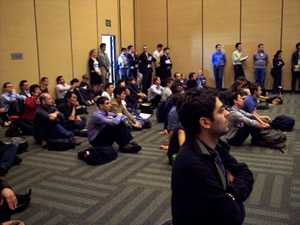
Standing room only in one of the presentations in Symposium R “Materials for Renewable Energy at the Society and Technology Nexus” of the 2009 Materials Research Society spring meeting (source: MRS)
For the electronic materials technologies that were the foundation of Silicon Valley, there were excellent updates on everything from high-k metal-gate (HKMG) transistors, to new 3D packaging materials, to thin-film transistors (TFT) for LCD, to non-volatile memory (NVM) cell technologies. The top electronics researchers in the world presented their most recent data to audiences of just 20-30 people, while around the corner it was standing-room only for talks regarding energy (see figure), the environment, or medicine.
Energy and the environment are clearly the main areas of interest these days. With 92 non-radioactive elements in the period table from which to draw, there are nearly endless combinations of compounds and nano-structures to test for new properties. Photoelectrochemistry may be used to generate hydrogen from sunlight and water. Shape-memory polymers may create artificial muscles. Any change of state in matter may be conceived of as the basis for a new IC memory cell.
IBM updated on porous low-k (PLK) dielectrics, H-P Labs updated on ReRAM (a.k.a. “memristors”), and RHEM and Ovonics updated on chemical-vapor deposition (CVD) of phase-change memory (PCM) materials. Both of the 2007 Nobel Laureates in Physics, Fert and Gruenberg for the giant magnetoresistive (GMR) effect used in hard-disk drives (HDD), presented as part of the symposium on spintronics. Details on these and other new electronic materials developments will be in upcoming BetaSights Newsletters. –E.K.
Tags: 32nm, 3D, CMOS, FPD, high-k, HKMG, IC, low-k, materials, memory, MEMS, NVM, PV, R&D, Si
Posted in fab, FPD, IC, MEMS, PV | Comments Off on MRS spring meeting beyond Silicon Valley
Thursday, April 16th, 2009
Abound Solar (formerly AVA Solar), a manufacturer of CdTe thin-film photovoltaic (PV) solar panels, announced the opening of its first full-scale production facility in Longmont, Colo. This facility uses a proprietary manufacturing process that is claimed to significantly reduce production costs of solar panels. The fully automated facility will create more than 300 new jobs and has ultimate planned capacity to produce 200 MW of solar modules annually.
 Abound Solar’s manufacturing process uses continuous in-line semiconductor equipment (see figure) to convert sheets of glass into solar panels in less than two hours. Abound Solar’s manufacturing process simplifies the production of thin-film solar panels, rapidly expands production capability and drives down the cost of solar-generated electricity. The company was founded in 2007 to commercialize 15 years of development at Colorado State University with support from the National Renewable Energy Laboratory.
“Today’s facility opening represents a milestone for Abound. We have moved into commercial production, which allows us to keep pace with demand from our customers as the market expands,” said Pascal Noronha, CEO of Abound Solar. “We are now well positioned to deliver high-performing, cost-effective, solar modules that can accelerate clean energy usage around the world.”
Unlike other CdTe fabs, Abound Solar’s process is fully automated, continuous, and uses dry deposition (though full details have not been disclosed). This results in claimed higher throughput, lower costs, and tighter process windows. The facility is fully integrated, converting glass and semiconductor materials into complete modules beneath its roof. At capacity, a glass panel will enter the factory every 10 seconds and emerge as a completed module two hours later. –E.K.
Tags: CdTe, fab, PV, solar, thin-film
Posted in fab, PV | Comments Off on Abound Solar opens first fab
Wednesday, April 15th, 2009
The first example of all-optical signal processing for communication above 100Gbit/s using silicon-based devices has been published in the April issue of Nature Photonics. Using deep-ultraviolet lithography, standard CMOS processing and organic molecular beam deposition, researchers from the University of Karlsruhe, IMEC and its associated laboratory INTEC at Ghent University, Lehigh University and ETH Zurich have now fabricated an innovative optical waveguide structure termed a silicon-organic hybrid (SOH).

Silicon-organic hybrid (SOH) optical waveguide (source: IMEC)
Today’s fiber-optic communication technology can transmit information across continents, but switching still requires converting the optical signals back to electronic data for processing. All-optical signal processing would overcome a serious bottleneck in such telecommunications applications, where speed, power and cost are crucial. An optical waveguide switch in which one light signal can direct the propagation of another would be a key element to enabling all-optical processing. However, while photonic technology can be ultra fast, the photon-photon interactions in known materials and structures has been too weak to be practical.
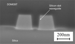
A 4mm long SOH waveguide proved the capability of the SOH concept (see figure). With these waveguides, all-optical demultiplexing of a 170.8Gbit/s telecommunication signal to 42.7Gbit/s was performed using four-wave mixing. This is the fastest silicon photonic optical signal processing demonstrated to date. In the four wave mixing process, a new wavelength is generated by combining the signal and control wavelengths. A dispersive coupling element can then separate this new wavelength and direct it to a different optical fiber. By pulsing the control wavelengths at a lower data rate than the signal, each compontent of a highly multiplexed signal can be selected. This experiment proved the viability of the SOH waveguides for all-optical processing of broadband telecommunication signals. More information on this breakthrough technology will be in the next BetaSights Newsletter. –M.D.L.
Tags: CMOS, DUV, IC, materials, Si
Posted in fab, IC | Comments Off on IMEC enables Si-based all-optical IC
Tuesday, April 14th, 2009
sp3 Diamond Technologies – the supplier of diamond film products, equipment, and services – today announced it is taking orders for 50mm and 100mm silicon on diamond (SOD) wafers for use as Gallium Nitride (GaN) substrates. Having worked with Nitronix on the GaN, sp3 Diamond Technologies uses combinations of thin-film depositions, wafer thinning, and layer transfer techniques to create SOD wafers that improve thermal conductivity compared to Si or SiC substrates. Work now is for the development of 150mm wafers for use as laterally diffused metal oxide semiconductor (LDMOS) substrates.
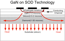
 100 mm SOD substrates were fabricated using hot filament diamond deposition on high resistivity float zone silicon wafers, followed by flipping and grinding the original substrate to create a thin silicon seed layer for the GaN epi layer. MOCVD technology was then used to grow the buffer, GaN and AlGaN device layers (see figure). Two different GaN layers were grown to investigate the effect on device performance as well as structural characteristics of the wafer. GaN devices layers were shown to be of sufficient quality to make HEMT transistors.
sp3’s SOD wafers deliver a high performance path for devices designed for WiMax base stations and other commercial and military broadband and high power switching applications. “High-power, high-frequency devices – such as high power radar and RF amplifiers, and DC to DC and AC to DC converters – have performance limitations due to the physical structure of standard silicon substrates,” said Dwain Aidala, president and COO of sp3 Diamond Technologies. “sp3’s SOD wafers deliver industry-leading performance, are scalable up to 300 mm and are available at a lower cost than alternative diamond-based solutions or traditional SiC substrates.”
The diamond heat spreading layer directly under the junction can allow for more than a 100% increase in power levels compared to silicon substrates alone, and a 50-80% increase when compared to SiC, at a fixed junction temperature. At fixed power, they can reduce junction temperature by more than 50 degrees compared to GaN on silicon or SiC. GaN growth on SOD reportedly yields epi films equivalent to GaN on silicon. –E.K.
Tags: 100mm, epi, GaN, HEMT, IC, LDMOS, materials, MOCVD, Si, SiC, SOD, thin-film, wafer
Posted in fab, IC, Material, Product | Comments Off on Silicon on Diamond 100mm wafers for GaN
Monday, April 13th, 2009
Intermolecular, the combinatorial R&D company that has been working on semiconductor fab processes, plans to grow solar R&D to possibly be the largest portion of the company’s business. Under the leadership of new vice president and general manager of solar business group Craig Hunter (who joined from Applied Materials), Intermolecular is now working on both silicon wafer and thin-film photovoltaic (PV) technologies. Surface texturing and various thin-film processes are the first immediate results shown.

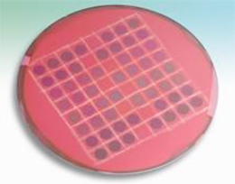
Combinatorial materials experiment for thin-film silicon PV cells; 56 unique transparent conductive oxides (TCO) plus controls on single substrate (source: Intermolecular)
“The first thing we do in any engagement is cross-correlate between our lab and the tool that would be used in production,” explained Hunter in an exclusive interview with BetaSights. Since Intermolecular has been working on 45nm node IC process integration, the company’s tools are capable of extremely tight process control. Most PV lines use tools with far less process control, and so the greater inherent variability in PV tools is one factor in the design of experiments (DOE). Using 300mm diameter glass wafers for combinatorial materials experiments, a thin-film deposition tool can perform 56 unique transparent conductive oxide (TCO) experiments along with the needed control experiments on a single substrate (see figure).
Hunter explained that a recent solar customer had consulted with them about the specifications for a critical inline process tool. There was a given non-uniformity across the cell, but it was not known quantitatively what improvement in overall cell efficiency might be achieved with a reduced non-uniformity. Intermolecular was able to quantitatively predict the efficiency improvement that would result, allowing the customer to justify an increased tool cost.
There are inherently unique PV requirements for homes, businesses, and utilities. Even for utilities, different technologies are needed to meet the different demands for large PV farms, distributed roof-top collectors, and building-integrated PV (BIPV). “The end makets themselves are not uniform in requirements, so having a technology platform that can contribute to each of these markets is exciting,” explained Hunter. More about combinatorial materials R&D for PV in the next BetaSights Newsletter. –E.K.
Tags: PV, R&D, Si, TCO, texture, thin-film, ZnO
Posted in fab, IC, Product, PV, Service | Comments Off on Intermolecular PV plans
 The Center at MIT is dedicated to inquiry, to dialogue, and to the creation of programs that affect the ethical and humane dimensions of life. This nonpartisan center is a collaborative think tank focused on the development of interdisciplinary research and programs in various fields of knowledge from science and technology, to education and international relations. The Center is founded to honor the vision of the Dalai Lama and his call for a holistic education that includes the development of human and global ethics.
