Friday, April 10th, 2009
The Materials Research Society (MRS) Bulletin for April 2009 covers some of the newest engineering work for the growth of large and pure electronic crystals. In this week before the annual MRS Spring Meeting in San Francisco, this issue of the monthly MRS members magazine provides an excellent overview of the latest technologies used to grow Si, Ge, GaAs, InP, as well as perovskite and other semiconductor crystals on industrial scales. The BetaBlog next week will be reporting from the San Francisco event.

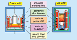
Traveling magnetic fields in Czochralski (left) and vertical Bridgman or vertical gradient freeze (right) crystal growth tools generated by heater-magnet modules (source: MRS Bulletin)
Industrial bulk crystal growth from the melt has gradually evolved in complexity to be able to ensure ever reduced costs and defect counts, typically through increases in size of the melt and crystal. However, larger melts display convective perturbations and even turbulences that produce large temperature fluctuations that induce growth rate oscillations seen as “striations” within the grown crystal. Melt convection non-uniformity may distort the melt-solid interface leading to higher dislocation density. Today’s state-of-the-craft for 300mm diameter Si growth uses traveling magnetic fields from heater-magnet modules (see figure) in both Czochralski (left) and vertical gradient freeze (VGF) (right) crystal growers.
Scheel and Schulz-DuBois (J. Cryst. Growth 8/304, 1971) introduced the accelerated crucible rotation technique (ACRT) for high-temperature solution growth. The technique has been used to grow a wide variety of crystals. In zone melting techniques from melt solutions, the ACRT enhanced the zone mixing and, therefore, the growth rate stepped up by approximately one order of magnitude. Recently, ACRT was used for the unidirectional solidification of photovoltaic (PV) multicrystalline silicon with improved carbon homogeneity and reduced impurity precipitates (Bairava Ganesh, et al., Cryst. Growth Des. 8/2525, 2008). ACRT transfers momentum from the crucible wall into the melt by modifying the rotation rate of the crucible as a function of time; the container accelerates from rest up to a maximum rotation rate followed by a deceleration or even a change in direction.
Among other articles, the issue also details recent progress in the growth of AlN and GaN crystals. The general problem of manufacturing low defect wafers of desired size is still an open issue. Physical vapor transfer (PVT) seems to be the best known method for AlN crystal growth, delivering dislocation densities as low as 1000/cm2 (100x improved from commercially available crystals today), but still requires a lot of tedious engineering work to increase the yield and scale the process beyond 25mm diameter crystals. Hydride vapor-phase epitaxy (HVPE) today provides modest quality GaN crystals, while improvements in quality and size up to 100mm diameter may be possible with the ammonothermal route under development by Ammono in Poland. More on crystal growing in the next BetaSights Newsletter. –E.K.
Tags: crystal, defect, epitaxy, GaAs, Ge, growth, IC, InP, PV, Si, wafer
Posted in fab, IC, Material, MEMS, Product, PV | Comments Off on Crystal growers and complex crucibles
Thursday, April 9th, 2009
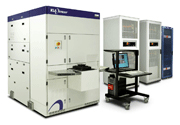
On April 7, 2009, KLA-Tencor introduced the TeraScanXR, the latest version of their TeraScan reticle inspection system, this one intended for 32nm node DUV masks. This new tool, an extension of existing reticle inspection systems, is designed to provide mask manufacturers better sensitivity, lower cost-per-inspection and faster mask dispositioning. Improvements in overall sensitivity in die-to-die and die-to-database modes meet 32nm requirements and allow pixel migration on less critical layers.
 The tools use high numerical aperture optics to inspect masks simultaneously in transmitted and reflected light at high-resolution – performing so-called reticle-plane inspection to capture a wide variety of defects. Then, using software, the TeraScan XR (see figure) computes how an exposure tool (with less resolution) would project the aerial image of that mask (aerial-plane inspection). Further computation can then infer the developed photoresist pattern that would finally appear on the wafer (wafer-plane inspection), helping to reduce the impact of non-printing nuisance defects that dominate in the “reticle plane.”
KLA-Tencor claims this to be the only reticle inspection tool on the market to supply the complete set of three “inspection planes.” Mask customers typically require every identified defect to be repaired and it remains to be seen whether they will accept evidence of the irrelevance of some reticle plane defects obtained by wafer plane computation. A substantial throughput improvement makes the XR version up to three times the speed of its predecessor, TeraScanHR, resulting in lower cost-per-inspection and enabling a mask set to be shipped to the fab in a shorter time.
Strong interest in the new system has resulted in several orders from the leading merchant and captive mask manufacturers in Asia and the United States, according to KLA-Tencor. As an upgrade on the industry-standard TeraScan 5xx platform, XR offers a cost-effective means to attain 32nm sensitivity for all reticle inspection applications. More on reticle inspection in the next BetaSights Newsletter. –M.D.L.
Tags: 32nm, DUV, IC, inspect, litho, mask, reticle
Posted in Equipment, fab, IC, Product | Comments Off on All-plane reticle inspection for 32nm
Wednesday, April 8th, 2009
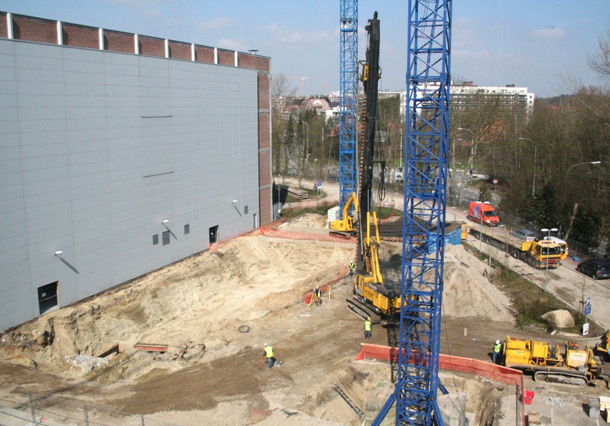
IMEC has begun expanding its beautiful Leuven, Belgium campus facilities, starting with 2,800 square-meters of research labs and including the extension of its state-of-the-art clean room. With this extension, IMEC will expand its research on 22nm CMOS and beyond, low-cost and high-efficiency solar cells, and biomedical electronics. The Flemish Government invests 35 million euro and IMEC will cover the remaining 35 million euro of the expansion through a loan. IMEC also plans to construct a new office building later, in this, its 25th year.
 Groundbreaking has started (see figure) on the 2,800 square-meters of extra lab space, which includes 1,200 square-meters of ultra-clean processing area as an extension of the current 300mm clean room. The new ultra-clean room will be “450mm-ready” so that IMEC’s advanced process technology research continues to follow industry standards. SEMATECH ISMI announced last fall that 450mm wafer handling tests have occurred, but factory interfaces are not yet set so probably the only fab spec. known today would be higher ceilings.
The remaining 1,600 square-meters of new lab space will be used to expand research on silicon and organic solar cells, and also on biomedical electronics. IMEC works on some of the major challenges of our planet: environment, energy, and the ageing population. Programs in areas such as solar energy, smart-grid, energy scavenging, and in several biomedical and medical applications address those challenges. Today, IMEC employs about 1650 people. With this expansion, IMEC expects to create about 300 new jobs in the coming years for many different profiles, including researchers, operators, and lab assistants in several domains.
Gilbert Declerck, CEO of IMEC, stated, “In 2009, IMEC lights 25 birthday candles. Thanks to the unbridled commitment of our researchers and the continuous vision and support of the government of Flanders, we succeeded in putting Flanders on top of the world in nanoelectronics research. We are proud that we can further expand IMEC’s activities so that we continue to offer valuable R&D programs to the industry that will contribute to Flanders, Europe, and the world of tomorrow.” –E.K.
Tags: 22nm, 450mm, CMOS, IC, organic, PV, R&D, Si
Posted in fab, IC, MEMS, Product, PV, Service | Comments Off on IMEC at 25 still growing
Tuesday, April 7th, 2009
Semiconductor Equipment and Materials International (SEMI) collects and reports market size information for key sectors of the semiconductor ecosystem. It recently issued figures for the materials market, which in 2008 totaled $42.7 billion, essentially flat with the prior year. According to SEMI, rapidly slowing economic conditions in the fourth quarter squelched prospects for year-over-year growth across the materials market.

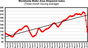
(source: SEMI Silicon Manufacturers Group)
At Semicon China 2009, SEMI president Stan Meyers presented a monthly wafer area shipment index that paints a picture of the dramatic shift in shipments in the final quarter of 2008 (see figure). As of January 2009, the index shows shipments have dropped from record levels in the middle of 2008 to average monthly levels not seen since 2002. (The SMG shipment numbers cover a broad range of products inclusive of polished silicon wafers, including virgin test wafers, epitaxial silicon wafers, and non-polished silicon wafers.)
Other materials followed a similar pattern. “Feedback we have received showed that sales and volumes started to crash in November, and December was disastrous,” recounted Mark Thirsk of the electronic materials research firm Linx Consulting. “ We have heard instances of zero monthly shipments in some supply chains.” From BetaSights’ point of view, these figures clearly indicate a correction and drawing down of inventories as opposed to a permanent shift in demand for materials. Thirsk agreed, “One thing is certain: inventories are now at rock bottom and below. Customer orders for materials are for days, not weeks, of supply.”
According to Dan Tracy, senior director of the SEMI Industry Research and Statistics group, wafer area shipment figures for February (the most recently available month) look about the same as January. There is good news, however. Unit shipments of leadframes, which in the second half of 2008 had tracked the dramatic decline of wafer shipments, showed an up tick in the February data. This is, we hope, the anticipated sign that we’ve reached the bottom of the current cycle. More materials numbers and analysis by Linx, Semico, and TechCet are in this week’s BetaSights Newsletter. –E.S.
Tags: CMP, Cu, IC, materials, Si, wafers
Posted in fab, IC, Material | Comments Off on Semiconductor fab materials market trends
Monday, April 6th, 2009
Applied Materials and Disco announced a joint effort to develop wafer thinning processes for fabricating through-silicon vias (TSV) for future 3D IC stacks. The two companies, world leaders in thin-films and thinning (respectively) for silicon wafers, will be working together to develop integrated, high-performance process flows intended to lower the cost, reduce the risk and accelerate time to market for customers’ next generation chips.

Applied Materials CMP, deposition, and etch tools used in TSV integration (source: Business Wire)
Combining Disco’s precision grinding equipment with Applied’s etch, dielectric deposition, physical vapor deposition and chemical mechanical planarization systems (see figure), the two companies expect to develop wafer thinning and post-thinning processes of wafers bonded to silicon and glass “handle” wafers. Nobukazu Dejima, president of Disco Hi-Tec America, said, “The capability to validate complete process flows using thinned wafers at our Santa Clara research laboratory and Applied’s Maydan Technology Center gives us a unique opportunity to exploit the advantages of thinned wafers in multiple TSV integration schemes.”
Not all chips today have to be ultra-thin, and the joint effort will work on a variety of targets for the final silicon thickness. “The final silicon thickness in the context of the announcement will be 30 to 200 microns, depending on the customer,” said Sesh Ramaswami, senior director of strategy for the silicon systems group at Applied Materials, to BetaSights. In addition to the possible use of plasma etch to remove post-grind backside damage, plasma etch in combination with thin-film deposition steps may also be used to develop integrated processes to engineer the backside structure of the exposed TSV. “The customer can’t really afford to do it,” explained Disco spokesman Scott Sullivan. Working together, Applied and Disco will share information, and hope to give customers a drop-in solution to the most demanded TSV process flows.
We’ll see 3D directions at the IEEE International 3D Systems Integration Conference (I3DSIC) that will occur in San Francisco for the first time, September 28-30. Abstracts are due May 15, with final papers by July 1st for this conference that combines the previous ASET/IEEE-EDS sponsored I3DSIC held in Tokyo in 2007 & 2008 and the IEEE-CPMT sponsored I3DSIC held in 2005 & 2007 in Munich. More on TSV technology and exclusive comments by Sullivan and Ramaswami will be in the next BetaSights Newsletter. –E.K.
Tags: 3D, Cu, DRIE, etch, IC, integration, TSV
Posted in fab, IC, MEMS | Comments Off on Applied Materials and Disco 3D TSV joint effort
Friday, April 3rd, 2009
The SPIE Europe Microtechnologies For the New Millennium congress has new partners this year, with the involvement of GMM, the Society of Microelectronics, Micro and Precision Engineering and the magazine mst|news as Cooperating Organisations for the first time. The event will be held at the Congress Centre Maritim Hotel in Dresden, Germany, 4-6 May 2009. “The interests of our respective audiences are similar, and we believe it will be of benefit to combine forces on this international conference,” said GMM executive director, Dr. Ronald Schnabel.
Plenary talks will be given by:
- Wolfgang Mueller of Qimonda Dresden, Germany, on “Future Memory Technologies;”
- Günter Lugert of Siemens, Germany, on EpoSS (the European Technology Platform on Smart System Integration;
- Griet Van Caenegem of the European Commission, Micro- and Nano Systems Unit, on “Microsystems and Smart Systems Technologies: A European Perspective;” and
- Jean-Michel Léger of CEA-LETI, France, on “Energy Harvesting and Power Management.”

Qimonda 65nm buried wordline DRAM chip (source: Qimonda)
Qimonda seemingly has some of the best DRAM technology for the future with it’s 4F² buried wordline technology (see figure). Work with Elpida was to take it to 45nm now and 32nm as the next step, but as of April 1st, the company is bankrupt. As of April 1st the company is bankrupt. A Munich-based lawyer continues as insolvency administrator for both Qimonda AG and Qimonda Dresden GmbH & Co. OHG companies, trying to find an “anchor” investor in a new Qimonda such that the fabs in Dresden, Munich, and Portugal remain to support as many jobs as possible.
About 600 employees in Munich (84%) and about 1,850 employees in Dresden (93%) accepted the offer made last week to join a transfer company on April 1, 2009. The transfer company guarantees the employees about 70 or 77% of the net wages that had been paid prior to insolvency. About 340 employees in Munich and about 575 employees in Dresden continue to work. Qimonda had invested liquidity for the development of its 46nm buried wordline technology in agreement with the creditors committee during the preliminary insolvency period. Now that work will continue at least until mid–August 2009. –E.K.
Tags: 32nm, 45nm, 65nm, DRAM, IC, MEMS, PV, SPIE
Posted in fab, IC, MEMS, PV | Comments Off on SPIE Europe Microtechnologies congress 2009
Thursday, April 2nd, 2009
The control of complex interdependencies is critical for the successful manufacturing of nanometer-scale ICs. Every aspect of every unit process step in the line must be ever more tightly controlled to ensure that 45nm and 32nm node chips can be made with good yield. To serve the market, Novellus continues to announce new integrated surface-treatment and deposition process-sets for dielectrics (Ref: BetaBlog 2009 March 20, and BetaSights Newsletter 2009 March 24), this time for barrier layers as thin as 10nm.

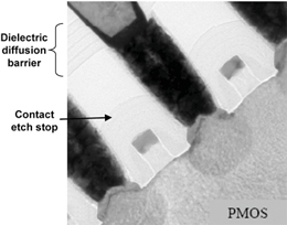
TEM cross section of a 65nm node device showing diffusion barrier and contact etch stop formed by multi-station sequential deposition (source: Intel)
The standard dielectric barrier material for 90nm and 65nm node interconnects has been nitrogen-doped silicon carbide (SiCN) with dielectric constant (k) of ~5. When integrated with a standard SiCO film of k~2.7, a SiCN barrier results in a k-effective of ~3.3 for the final stack. To reach a target k-effective of ~3.0, there are two basic approaches: lower the k value of the barrier with a new material, or else thin the barrier with the same material. A new material requires new integration work, so it is easier to stay with SiCN if it can be done. Novellus has shown that the laminate/multi-layer films (see etch decorated layers in figure) deposited in multi-station sequential processing (MSSP) tools can meet barrier specs despite less mass per area.
Taking advantage of interface and bulk film controls afforded by MSSP, Novellus researchers have successfully demonstrated that 25nm SICN can replace 50nm of the barrier material. “Novellus’ diffusion barrier films meet today’s performance needs and have been demonstrated to meet the EM and dielectric breakdown requirements for future technology generations,” said Kevin Jennings, senior vice president and general manager of the PECVD business unit. The company claims that the line-to-line leakage (extacted at 2MV/cm) was essentially identical at the bottom of the instrument detection limit for stacks using the SiCN barrier at thicknesses of 70, 50, and 10 nm.
“Thinning dielectric barriers is an approach that has been used by several IC manufacturers in the 65-45nm transition,” explained Mandayam Sriram, Director of Technology for PECVD. “This approach for sub-45nm technology nodes is challenging and alternate approaches are being considered. We now have a viable, demonstrated HVM solution for sub-45nm technology nodes with the low risk, thinner barriers that provide the RC scaling requirements and at the same time meet the EM and TDDB requirements.” More exclusive comments from Sriram about dielectric integration will be in the next BetaSights Newsletter. –E.K.
Tags: 32nm, 45nm, 65nm, barrier, CVD, IC, low-k, PECVD, SiCN
Posted in Equipment, fab, IC, Product | Comments Off on Novellus 32nm dielectric barriers
Wednesday, April 1st, 2009
Asahi Glass is promoting a family of new photosensitive spin-on-dielectric (SOD) films for fan-out WLP and 3D packages, as well as for FPD and MEMS applications. The Chemicals Fluoroproducts Division of Asahi Glass has successfully developed the AL-X polymer series, primarily targeting the redistribution/rewiring layers in fan-out WLP packages. The company will begin production of the AL-X fluoropolymer dielectric precursor at its Chiba Plant (Japan), with marketing operations of the product already started in January 2009.
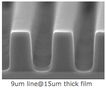
 Mechanical properties of the final film include elongation of 20% and Young’s modulus of 1.3GPa, so this is a relatively soft and “rubbery” dielectric. The dielectric constant (k) is 2.6-2.7 (@1MHz-1GHz). The precursor is formulated in different viscosity blends so that three different final film thickness ranges can be achieved: 1.5-3.5µm, 3.5-10µm, and 8-30µm. Using the thickest viscosity spun to 15µm film thickness, 9 µm lines and spaces have been patterned with decent sidewall angles (see figure).
The precursor reportedly planarizes quite well over micron-scale topography. The basic process flow after spin coating the polymer is as follows:
• Soft bake for 90s at 80C,
• Expose with i-line using negative mask,
• Develop and rinse in solvent, and
• Hard bake at 180-250C.
Integration work on WLP using this material will be done by Asahi Glass in cooperation with RTI International in Research Triangle Park, North Carolina (U.S.) which has successfully developed processing guidelines for the new dielectric film. The material may also see use as a wafer bonding material for MEMS, and there is also a high transparency version for application as the interlayer dielectric for flat panel displays (FPD). More on spin-on dielectrics in the next BetaSights Newsletter. –E.K.
Tags: 3D, FPD, IC, litho, low-k, Material, MEMS, package, photo-SOD, SOD, spin-on, WLP
Posted in fab, FPD, IC, Material, MEMS, Product | Comments Off on Asahi Glass photo-SOD
Tuesday, March 31st, 2009
Semilab, founded in 1990 and headquartered in Budapest, Hungary, is spending cash to continue to expand its portfolio of fab metrology offerings. Today, the company announced it has acquired Advanced Metrology Systems (AMS) and QC Solutions. The two Massachusetts-based metrology companies expand Semilab’s family of scalable, flexible solutions to help semiconductor and solar manufacturers characterize materials. Semilab claims an installed base of over 3000 metrology systems worldwide.

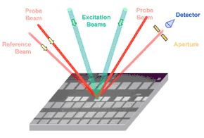
Dual-beam surface acoustic wave metrology for measuring Cu post-ECD (source: Semilab AMS)
AMS offers solutions for fast and detailed characterization of 3D etched structures including contacts and trenches using model-based IR (MBIR) technology; metal film thickness on product wafers using acoustic surface wave profiling (see figure); and high speed online mapping of low-k material properties. AMS’ award-winning products are installed in the fabs of IBM and AMD. AMS will now become part of a Massachusetts division of Semilab known as Semilab AMS. QC Solutions offers patented, non-contact, non-destructive systems for the fast and repeatable measurement of the electrical properties of epitaxial and implanted silicon wafers. QC Solutions will also become part of Semilab AMS.
“With these acquisitions, we are expanding our ability to provide a full set of metrology solutions to support basic material characterization in everything from R&D settings to fully automated production lines,” said Dr. Tibor Pavelka, one of the founders, now president and CEO of Semilab. “We believe investing in the semiconductor market, even in these tough times, will enable us to continue our nearly 20 years of growth and profitability and meet the metrology needs of the market presented by the drive to smaller nodes and new materials.”
Both acquisitions were all cash transactions. QC Solutions and AMS are the latest metrology companies to be acquired by Semilab. In 2008, the company purchased the assets of French metrology equipment specialist Sopra. In 2008 Semilab acquired the majority of SSM of Pittsburgh, PA, and the Boxer Cross metrology IP from Applied Materials. Semilab also started a JDP with IMEC for high-k dielectric metrology last year. More about specialty metrology in the next issue of the BetaSights Newsletter. –E.K.
Tags: 45nm, epi, fab, high-k, IC, implant, Material, metal, metrology, PV, solar, test, thin-film
Posted in Equipment, fab, IC, MEMS, Product, PV | Comments Off on Semilab acquires AMS and QC Solutions companies
Monday, March 30th, 2009
The principles of “causality” and “boundary conditions” are fundamental to modern science, and when you apply these principles to the system of human energy production/consumption it tends to lead to thoughts of TeraWatt Challenges and limiting demand. Raw energy limits need not equate with lifestyle limits, if new technologies allow us to be far more efficient with our natural abundance of resources. However, needed changes require global support, so hundreds of millions of people around the world joined in a symbolic gesture by turning off their lights for one hour March 28th.
 World Wildlife Fund (WWF), the world’s largest multinational conservation organi- zation, organized “Earth Hour” to be observed by switching off all of your electric lights for one hour starting at 8:30pm (20:30-21:30) in your local time zone. Though not reaching the goal of 1 billion people, the organizers claimed that it was observed in more than 3,900 cities in 88 countries, with promotional help from sponsors including Hewlett-Packard. Lights were out at the Golden Gate Bridge in San Francisco, the U.N. building in New York City, the pyramids in Egypt, the Beijing Oympics stadiums, and the Oriental Pearl Tower in Shanghai (see figure).
Earth Hour was celebrated as it cascaded through the world’s time zones. Individuals, villages, towns, major cities, organizations and corporations, and the world’s most recognizable landmarks, all united in a truly global effort. BetaSights headquarters turned off the electric lights and lit a few candles.
“As the world witnessed Saturday night, the simple action of turning off lights can inspire people around the world to take action, and to make a serious long-term commitment to living more sustainable lives,” said WWF President and CEO Carter S. Roberts. “On behalf of WWF, I want to thank all participants for making Earth Hour a truly memorable hour for the entire planet.” We can all act to be more energy efficient, more carbon neutral, and more globally responsible. More on energy technology and efficiency in the BetaSights Newsletter. –E.K.
Tags: PV
Posted in FPD, IC, MEMS, PV | Comments Off on World thinks about Earth for one hour
