Friday, March 27th, 2009
Materials research and engineering continues to increase in structural complexity. Starting from the periodic table of the elements and molecular engineering, over a century of research has explored most obvious phenomena of bulk and thin-film materials. What, then, is left to explore? The vast complexity of natural micro- and nano-scale structures that are indirectly templated by DNA in living organisms. From gecko toes to lotus leafs, bio-inspired researchers have found that studying what nature has evolved points the way to fabricating new functional materials. Georgia Tech researchers used DARPA money to copy and improve on the flow-sensing hairs of the blind cave fish, and talked about it at the American Physical Society meeting on March 20.

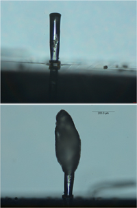
Synthetic hair sensor before and after coating with a hydrogel material (source: Georgia Tech researcher Michael McConney)
The blind fish have evolved sparse body hairs that are highly sensitive to the movement of water. “The fish can detect flow slower than 100 micrometers per second, but our system demonstrated flow detection of several micrometers per second,” said Vladimir Tsukruk, a professor in the Georgia Tech School of Materials Science and Engineering who led the work. The researchers knew that the fishy hairs were sensitive, so measuring the hairs with optical and confocal fluorescence microscopy allowed them to set initial size, aspect-ratio, and surface complexity parameters for experiment. The synthetic hairs are formed from a core of standard SU8 photo-epoxy used in MEMS and packaging fabs, then coated with a “cupula” of a UV-cross-linked hydrogel (see figure).
“These hair cells are like well-engineered mechanical sensors, similar to those that we use for balance and hearing in the human ear, where the deflection of the jelly-encapsulated hair cell measures important flow information,” said Vladimir Tsukruk, a professor in the Georgia Tech School of Materials Science and Engineering. “The hairs are better than active sonar, which requires a lot of space, sends out strong acoustic signals that can have a detrimental effect on the environment, and is inappropriate for stealth applications.” If this can be scaled up to Navy specs, then the sensitive ears of whales and dolphins could be saved from active sonar.
To date, the researchers have fabricated an array of eight microsensors and shown that the array is able to detect an oscillating object underwater. They are currently looking for industrial partners to efficiently scale-up the research by fabricating arrays of thousands of these sensors and testing them in real marine environments. The synthetic hairs are in the 0.5-0.8 mm tall range, so many different fab technologies already developed for IC/MEMS packaging using SU-8 could potentially be used. More on synthetic blind fish hairs in a future BetaSights Newsletter. –E.K.
Tags: materials, MEMS, package, R&D, sensor, SU-8
Posted in fab, Material, MEMS | Comments Off on Blind fish hairs inspire flow sensor
Thursday, March 26th, 2009
German and French teams are combining EUR 14.5m investment into development of strained-silicon on insulator (sSOI) technology under the DEvice and CIrcuit performance boosted through SIlicon material Fabrication (DECISIF) program. The work will combine original research results from Research Center Juelich and Leti/Soitec to try to lower costs and defect-densities in the creation of 300mm sSOI wafers for microprocessors and consumer systems-on-chips. Work will start on 45nm node structures, with extension to 22nm planned.

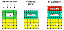
Cross-sectional schematic of sSOI key process steps (source: Research Centre Juelich)
The Federal Ministry of Education and Science (BMBF) granted EUR 8.1m for DECISIF Another EUR 6.4m will be contributed by the project partners GlobalFoundries Dresden, Siltronic, Aixtron, Research Center Juelich, and the Max Planck Institute of Microstructure Physics. French partners STMicroelectronics, Soitec, and Leti will also collaborate within the scope of the EU-project Medea. Prof. Siegfried Mantl of Research Center Juelich, the project coordinator for Germany, told BetaSights that they will investigate strain/stress on the wafer level (see figure showing the “Juelich process”) as well as on the transistor level with new stressor methods.
The Juelich process starts by growing a cubic-Si/strained SiGe/Si heterostructure. Then, the pseudomorphic SiGe layer is relaxed using a He+ implantation and an annealing step. The relaxation of the SiGe layer establishes the elastic strain in the top Si layer. The strain generated depends on the layer thickness and the degree of relaxation of the SiGe layer. For top Si thicknesses up to 8 nm (over 150 nm thick Si0.74Ge0.26), 100% strain transfer is observed.
These global strain techniques will be combined with new techniques to create locally strained silicon to reach an exceptionally high mobility of the charge carrier within transistors. The objectives of this project are to integrate performance boosters in fully- and partially-depleted SOI for Low Power and High Performance, to validate these technologies by fabricating complex 45nm node demonstrators directly comparable with bulk Si and to develop design kits and SOI-adapted circuit design for evaluation by application designers. More on sSOI and exclusive comments from Mantl will be in the next BetaSights Newsletter. –E.K.
Tags: 22nm, 32nm, 45nm, CVD, EDA, epi, IC, implant, integration, Material, Si, SiGe, SOI, sSOI, strain, wafer
Posted in fab, IC, Material, Product | Comments Off on DECISIF start on strained silicon
Wednesday, March 25th, 2009
Novaled, the provider of Organic Light Emitting Diode (OLED) technology and materials, and Holst Centre, an independent R&D centre developing generic technologies for Wireless Autonomous Transducer Solutions and for Systems-in-Foil, have decided to collaborate on the development of organic thin film transistor (OTFT) technologies under a joint development agreement. Novaled will provide its organic dopants to the Holst Centre for applications as displays and circuits.

CMOS organic TFT (OTFT) cross-sectional schematic (source: Novaled)
Novaled’s doping technology contributes to very high power efficiencies and long lifetimes in OLEDs by improving charge carrier injection and transport in the organic layers. These effects are also relevant for OTFT devices, as the carrier injection from drain and source into the organic material has a major influence on the device performance. Novaled currently develops dopant and host materials which can be processed both in vacuum and in solution.
”In the future, OTFTs can be integrated in display backplanes and other driving electronics like organic RFID (radio-frequency identity) tags,” said Jan Blochwitz-Nimoth, CTO of Novaled. With the potential for easy and low-cost manufacturing, OFTF could change the way we use electronics today. The challenge has been in finding the right combination of specialty materials that can be printed across large areas.
Gerwin Gelinck, Program Manager Organic Circuitry at Holst Centre, commented, “It is our strong believe that only through this type of collaboration, cutting edge processes and prototypes are developed that will accelerate introduction of organic transistor products to the market place. For the other Holst Centre partners in our Shared Program the joint development project with Novaled offers a unique opportunity to evaluate the potential of this approach at first hand.” More on OTFT in the next BetaSights Newsletter. -E.K.
Tags: CMOS, dopant, IC, Material, OLED, organic, OTFT, TFT
Posted in fab, FPD, IC, Material, Product | Comments Off on Novaled and Holst Centre JDA on OTFT
Tuesday, March 24th, 2009

A solar prominence unfurls in this image of extreme ultraviolet light emitted by He ions (source: NASA; http://antwrp.gsfc.nasa.gov/apod/ap081004.html)
It is always sunrise somewhere on our spinning sphere, and the sun is always changing too (see figure). There are always ups and downs in our world, and we learn to “make hay while the sun shines.” Where has the sun been shining lately? Photovoltaic (PV) and MEMS industries have continued to grow lately, as have the fortunes of companies suppplying technologies to these lines.
Steven Chu, the new U.S. Energy Secretary, is reportedly scrambling to hire experienced staff to help him spend tens of US$ billions in alternative energy stimulus dollars. The twin goals are to stimulate the economy in general, and to develop new technologies that could lead to energy independence. On March 20th, Solyndra announced that it is the first company to receive an offer for a U.S. Department of Energy (DOE) loan guarantee under Title XVII of the Energy Policy Act of 2005. Solyndra will use the proceeds of a $535 million loan from the U.S. Treasury’s Federal Financing Bank to expand its solar panel manufacturing capacity in California.
The guaranteed loan, expected to provide debt financing for approximately 73% of the project costs, will allow Solyndra to initiate construction of a second solar panel fabrication facility (Fab 2) in California. On completion, Fab 2 is expected to have an annual manufacturing capacity of 500 megawatts per year. Solyndra estimates that the construction of this complex will employ 3,000 people, the operation of the facility will create over 1,000 jobs, and hundreds of additional jobs will be created for the installation of Solyndra PV systems, in the U.S.
BetaSights recently visited Xactix in Pittsburgh, PA, and the MEMS OEM reports booming business for Xenon difluoride (XeF2) chemical vapor etch (CVE) systems. The rumor mill in Silicon Valley reports that GlobalFoundries is hiring staff. Though Global Foundries’ major fab is in Dresden, Germany, and major funding is in Abu Dhabi, the spin-out’s headquarters is in Sunnyvale, California so that’s where the new staff will likely sit. More about sunrises in this week’s BetaSights Newsletter.—E.K.
Tags: CIGS, fab, MEMS, PV
Posted in Equipment, fab, MEMS, Product, PV | Comments Off on Always sunrise somewhere
Monday, March 23rd, 2009
Keithley Instruments has been very busy extending the capabilities of it’s 4200-SCS (Semiconductor Characterization System) with new cables for IC measurements and new software libraries for PV, OLED, and other devices. The 4200-SCS replaces a variety of electrical test tools with a single integrated characterization solution, and works for applications including semiconductor technology development, process development, and materials and device research labs. The test systems’s modular architecture allows for easy field upgrades, like those just released.

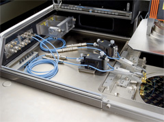
Triaxial cable allows for I-V, C-V, and pulsed I-V tests (source: Keithley Instruments)
The new triaxial cabling kits (see figure) are based on a patent-pending design that speeds and simplifies the process of making DC Current-Voltage (I-V), Capacitance-Voltage (C-V), and pulsed I-V testing connections. The new cables connect any modern semiconductor parameter analyzer to a Cascade Microtech or SUSS MicroTec prober, and allow for switching between measurement types without recabling. In addition, test setup changes can be made while the probe needles are in contact with a wafer, reducing pad damage and maintaining the same contact impedance for all three types of measurements. The cables are designed for compatibility with the 4200-SCS, as well as with other test instruments.
The company has introduced other hardware, firmware, and software enhancements to the 4200-SCS. The Keithley Test Environment Interactive (KTEI) V7.2 upgrade includes nine new solar cell test libraries, an expanded frequency range for the system’s C-V measurement capability, and support for the company’s new nine-slot Model 4200-SCS instrument chassis.
The new test libraries expand capabilities for solar cell I-V, C-V, and resistivity testing applications, and also supports Drive-Level Capacitance Profiling (DLCP). Lowering the frequency range to 1kHz (from the previous 10kHz) provides for testing of LCDs and organic semiconductors such as organic light-emitting diodes (OLEDs), and also allows for DLCP. DLCP of thin film solar cells was first shown by Michelson et al. in 1985, but can result in erroneous defect densities if test parameters are not proper. Version 7.2 of KTEI is available at no cost to existing 4200-SCS users. More about test in the BetaSights Newsletter. –E.K.
Tags: C-V, characterization, FPD, I-V, IC, OLED, prober, PV, Semiconductor, test
Posted in Equipment, fab, FPD, IC, MEMS, Product, PV | Comments Off on Keithley 4200-SCS upgrades
Friday, March 20th, 2009
Novellus’ applications labs have been working on CVD low-k dielectrics targeting 32nm node multilevel metal specs, and the result is “dense” ultra-low-k (ULK) film with bulk k=2.5 and the potential to go lower. Combined with the company’s multi-station sequential processing (MSSP) tool architecture for the barrier/cap depositions and UV/thermal cure steps, the result is a claimed 5% reduction in the effective k compared to porous low-k (PLK) films. With complex interdependent trade-offs in interconnect materials today, there are inherent complexities in the solutions as well as in the descriptions of those solutions. To discuss such complexities, instead of a one-time press release the company has launched a new technology information page on online.

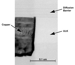
Single-phase ULK dielectric integrated with Cu dual-damascene interconnect (source: Novellus)
Despite mis-directions from early editions of the ITRS, in which a new low-k material was supposed to be integrated into production for each new node, the world has mostly settled on the use of CVD SIOC(H) for k~3 films. To be sure, successively lower capacitances would have nicely lowered the RC delay factor in interconnects, but new materials have been difficult to find and expensive to integrate. In particular, dielectric barrier and etch-stop layers require relatively higher k value such that the effective k for the whole dielectric stack (see figure) is always greater than that for the main low-k film alone. “RC scaling is about k-effective, not the absolute k value of each layer,” reminded Mandyam Sriram, director of technology for Novellus’ PECVD business unit.
“We don’t think that it’s important to compete on the marquee value of bulk low-k. We’ve taken a different approach,” said Tim Archer, executive vice president of the PECVD business unit, in an exclusive interview with BetaSights. “Most of our competitors have been working on PLK in the 2.3-2.4 range. We think that we can deliver a full stack that will rival or beat the k-effective of the PLK.” The barrier layer depositions and UV cure steps really can make or break k-effective.
The company’s “dense” ULK film is reportedly deposited as a single phase from a single precursor, instead of the two precursors used for PLK deposition. Still, the ULK material requires a cure step that outgases some material, and data shows the material’s k value reducing along with density. The company officially has no comment on comparisons between its ULK and the molecular pore stack (MPS) ULK shown by NEC (Ref: BetaBlog 090317). More exclusive info on low-k dielectric integration and Novellus’ plans will be in the next BetaSights Newsletter. –E.K.
Tags: 32nm, 45nm, cure, CVD, IC, low-k, MPS, PLK, ULK, UV
Posted in Equipment, fab, IC, Product | Comments Off on Novellus low-k integration ideas
Thursday, March 19th, 2009
Mentor Graphics has announced new capabilities to the Calibre(R) platform to allow designers to control thickness variability due to Chemical Mechanical Planarization (CMP) at advanced process nodes. Designers can transition from dummy fill to density-based fill, or to full model-based fill, depending on the demands of their designs and target manufacturing process. The new capability comes from combining the company’s Calibre litho modeling with the CMP sensitivity modeling acquired with Ponte Solutions last year.

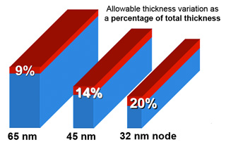
Allowable thickness variation post-CMP remains +-10nm so the percent variation increases for each node; model-based fill techniques minimize such variations (source: ITRS)
Variations in thickness created by chemical-mechanical processing (CMP) can lead to manufacturing and parametric performance issues. Metal “fill” attempts to achieve an even distribution across the die by adding non-functional metal shapes to “white space” regions in a design. However, adding too much fill can increase parasitic capacitance. We need fill in the right places to optimize performance while minimizing manufacturing variations. Because the percentage of total thickness variability per layer has increased at each node (see figure), CMP variations are much more significant below 65nm, and traditional dummy fill approaches are no longer adequate.
Both AMD and CSR have already used SmartFill; CSR was able to successfully tape-out a RFCMOS 65nm design and get first-time-right working chips from TSMC. Achieving even greater accuracy requires detailed simulation of the CMP process, and so Calibre now provides its own CMP simulator with models for leading fabs validated against silicon. Because the rapidly changing CMP process often requires model updates, it allows users to create and calibrate their own thickness models, a capability that is unique in the industry. “Today Mentor Graphics is announcing the availability of a CMP model specifically calibrated to Chartered Semiconductor’s 45nm process,” stated Walter Ng, Vice President of Design Enablement Alliances at Chartered Semiconductor Manufacturing.
“We already have 10 to 20 companies working with us on SmartFill,” said Michael Buehler-Garcia, director of Calibre Design Solutions Marketing, formerly of Ponte Solutions (and formerly of PDF Solutions where this editor reported to him). More about DFM and CMP, from exclusive interviews with Buehler-Garcia and CMP guru Michael Fury will be in the next BetaSights Newsletter. –E.K.
Tags: 45nm, 65nm, CMP, EDA, fill, IC, metal, model, variation
Posted in fab, IC, Product, Service | Comments Off on Mentor 3D solves CMP variation
Wednesday, March 18th, 2009
Wright Williams & Kelly (WWK), the cost and productivity modeling company, is now providing free general information in an electronic newsletter, and has lowered the cost to start using it’s flagship TWO COOL(R) cost of ownership (CoO) modeling software. The company’s “Applied Cost Modeling” newsletter features free excerpts from the book “Hi-Tech Equipment Reliability: A Practical Guide for Engineers and Managers.”

TWO COOL V3 provides GUI with simultaneous data entry and results panels (source: WWK)
The CoO and overall equipment efficiency (OEE) modeling software, now version 3 (see figure), is the de facto standard for fab industries, since it was derived from original SEMATECH CoO modeling work and is compliant with SEMI standard E35. Previously, the software was licensed with a minimum of 10 seats. Through the end of May 2009, the company is offering a 1-seat license for $4,995, including free attendance at a training which will be held at SEMICON West/InterSolar 2009 on July 16 at the San Francisco Marriott. The company also offers a 1-seat license to qualified universities for just $495.
“It has been over a decade since we offered a 1-seat license to TWO COOL,” stated David Jimenez, WWK’s president. “However, this is the ideal time for our clients to invest in improving their cost competitiveness, and WWK is dedicated to helping them achieve these goals with the smallest cash outlay possible.” It is incredibly useful and flexible for anyone working with high-tech manufacturing technology. However, as with any flexible modeling tool it is utterly essential to have proper inputs, so take the training if you license a seat.
This editor has been working productively with versions of this software since 1992, and used it to model the integration costs of different low-k dielectric technologies for a Materials Research Society presentation in 1997 (Session N3.10). For the last 12 years, CVD SiOC has been the dominant low-k dielectric, as predicted by the cost model. More about CoO, as well as the right way to estimate real fab costs for different tools, will be covered in the next BetaSights Newsletter. –E.K.
Tags: CoO, fab, FPD, IC, MEMS, model, OEE, PV
Posted in fab, FPD, IC, MEMS, Product, PV, Service | Comments Off on WWK cost modeling tools
Tuesday, March 17th, 2009
Breaking news about a leading porous low-k (PLK) material from Japan was first revealed in the SemiNeedle Planarization Lounge Forums (www.semineedle.com/forums/5001) about two months ago. During an expert panel discussion on CMP integration with low-k materials (moderated by this editor, summarized in “Chemical-Mechanical Planarization (CMP) technology consensus 09Q1” publication available at the site), Dick James, of reverse-engineering expert firm ChipWorks, disclosed that he had recently seen the first use of a PLK in a commercial chip his company had examined. Fujitsu is now fabbing Via Technologies’ new Nano CPU for “surfbored” (joke spelling intentional) notebooks, using nano-clustering silica (NCS) PLK of k~2.3.

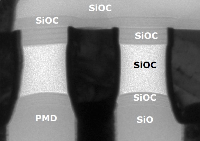
Via Technologies Nano CPU interconnect cross-section, fabbed by Fujitsu, showing use of NCS porous SiOC between caps of dense SiOC (source: ChipWorks)
There are many known integration challenges with PLK materials: material degradation during plasma etch, pore-sealing on sidewalls, compatibility with metal CMP processes, etc. In particular, for CMP most workable integrations use a capping layer of another dielectric such as standard CVD SiOC or a spin-on undoped silicate glass (USG). The Via Nano chip fabbed by Fujitsu shows NCS capped with a layer of CVD SiOC according to ChipWorks (see figure).
In Session 26.7 of IEDM2008, NEC showed “damage-less” full Molecular Pore Stack (MPS) SiOCH intermetal dielectric integration including direct CMP. MPS thin films are formed from ring-type siloxanes (with high carbon content) in CVD chambers, resulting in dielectric k=2.5 and resistance to plasma-induced damage. With small average pore size (<1 nm) there is low potential for water-absorption with MPS films, and having smaller pores reduces intrinsic line edge roughness (LER).
The bulk MPS material is hydrophobic so that an aqueous process like CMP leaves water marks behind. NEC experimented with He plasma treatment to alter the MPS surface, and found that 15 seconds reduces carbon to make the surface hydrophillic, but treatment for >30 seconds tends to form a top crust which cracks and shows as scratches. Using a He-plasma treatment in the 15-20 seconds range is thus key to cost-effective integration of MPS in dual-damascene Cu flows. The company claims that there is margin for overpressure in CMP using this dielectric without a cap. Full details about these development are in the latest BetaSights Newsletter. –E.K.
Tags: cap, CMP, dielectric, IC, interconnect, low-k, MPS, NCS
Posted in fab, IC, Material, Product | Comments Off on Low-k MPS and NCS updates
Monday, March 16th, 2009
The BetaBlog of March 5th was originally titled “Amkor chooses TMV not TSV for PoP” and Amkor’s stalwart vice president of business development Lee Smith contacted BetaSights to correct the impression that Amkor may have chosen to not work on TSV. I’d intended the original title to be somewhat playful; since TSV is chip-level while TMV and PoP are of course inherently package-level technologies, the title called into question when TSV might be used in place of PoP. The title has been changed to “Amkor’s TMV PoP will go to 0.3mm.”
The graphic shown in the March 5th post was a schematic of a TMV PoP using wire-bonded chips. However, the TMV package can just as easily handle chips with TSV. “If you needed high density, you could combine TSV and TMV to achieve very hgh density stacking,” explained Smith. “It’s not a straight approach to choosing one or the other.” What about functional overlap between TMV and so-called “2nd-generation” TSV with ~100 embedded conductors? Smith insists that the technologies are completely complementary.

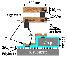
Edge connection over 100 micron thin silicon chip (source: Tohoku University)
Amkor’s motivation with TMV is to provide a low-risk path to extend PoP for it’s customers. “They want to maintain the current SMT infrastrucure, so a new bottom package technology was needed,” explained Smith. In the next 12-14 months, low-power DDR2 is being specified for stacking on top of mobile processors, and the bottom package to memory package interface for some will drop from 0.65mm to 0.5mm or 0.4mm pitch according to Smith.
Besides PoP and TSV, the other known 3D stacking solution is edge-contacts (see figure, shown by Tohoku University in Session 20.5 of IEDM 2008). While certainly providing unique capability, the cost/performance of edge-connnections has always limited such approaches to niches like Mil/Aero. Thus, while edge-connection technology exists, it must win competiton with wire-bond, flip-chip, and now TSV, and that may be difficult. –E.K.
Tags: 3D, IC, memory, PoP, TMV, TSV, WLP
Posted in fab, IC | Comments Off on Amkor TMV also for TSV
