 |
|
| Password: | |
 |
 |
 |
 |
 |
 |
 |
 |
|
|
Company Profile BetaSights (www.betasights.net) is a new information service—launched by industry veterans Ed Korczynski and Elizabeth Schumann in 2009—that provides commercial free, member supported, productive info about micro- and nano-device manufacturing. Covering the leading edge of fab technologies for ICs, MEMS, FPDs, and PVs, BetaSights focuses on the customer beta evaluations of new equipment, materials, processes, and services that occur after alpha R&D but before volume production. Our Shared History It has been said that, "we are dwarfs standing on the shoulders of giants." High tech is the same. Fabrication technologies are rarely utterly novel, but almost always targeted applications in unique directions starting from known developments for other applications. M. David Levenson's 1982 invention of the phase-shift mask enabling sub-wavelength lithography was a rare exception. Sometimes giants do stand on the shoulders of giants, and see the need for new materials. The history of tungsten wire production is illustrative of just some of the complexity involved in materials engineering. Then, specialized materials are processed in specialized equipment to make new micro- and nano-devices in fabs today at the limits of human knowledge. 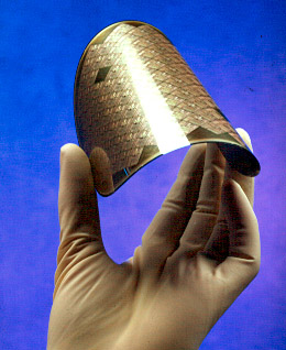 Device fab technology is incredibly complex, relying upon the careful coordination of numerous nuanced engineering disciplines: materials, electrical, chemical, mechanical, optical, etc. Each area of expertise is built upon thousands of years of science and engineering developments, and when it all comes together it can seem miraculous. Watch the intensely vivid colors of a plasma glow and dance inside an etch chamber as pressure, energy, and ion flow change. Feel the single-crystal silicon of a 50µm thin wafer elastically flex in your hand without breaking when surfaces have been etched clean of all damage (see figure, 1999 Ed Korczynski's hand). See a scanning-electron microscopic image of a 45nm IC feature printed with a 193nm laser--the wavelength four times wider than the line. Bubble unnatural gases through incredible liquids and nano-scale dust particles form that glow when you run electricity through them. Amazing functionalities can be made in micro- to nano-scale forms...all relatively inexpensively when done on huge industrial scales.
With a solid half-century of experience, a treasure trove of tricks are known to carve crystals and melt metals. Some have been written down, but all started as part of a strict oral tradition (despite lab notes). In a culture that loves TLAs (three letter acronyms), this empirical oral tradition's developments are called POR (processes of record) that use BKM (best-known methods) involving SMS (specialty materials suppliers) and OEM (original equipment manufacturers). Proven processes rely upon proven materials and proven tools, and rigorous DOE (design of experiments) sets in manufacturing test anything new that comes from a development lab. After a technology passes lab alpha tests to show proof of concept, it must undergo beta tests at a real fab site to show proof of repeatability, cost-of-ownership (CoO), and most essentially the yield. In nano-scale IC fabs, it can cost over US$1M in wafers and labor and fab use to thoroughly test a new technology developed by a supplier. It is both an honor and the last great hurdle for a new technology to be installed on the floor of a working fab, whether pilot or high volume. BetaSights provides insight into the beta sites of fab technologies, tracking new materials, equipment, processes, and services that are now being evaluated for commercial applications. Who We Are Ed Korczynski, Founder and Editor  Ed Korczynski has worked in the micro- and nano-device manufacturing ecosystem since receiving his degree in Materials Science and Engineering from MIT in 1984. He was a process engineer in IC, opto-electronics, and MEMS fabs, and developed custom tools and recipes. He managed applications and products for semiconductor OEMs from start-ups to stalwarts, and directed international joint-venture technology developments. As an award-winning technical editor for Solid State Technology magazine, he wrote the popular weekly blog Ed’s Threads from 2006-2008. He is a member of the Materials Research Society. edk@betasights.net Elizabeth Schumann, Principal Analyst  Elizabeth Schumann has over 20 years experience conducting industry research and analysis in semiconductor equipment and materials, FPD, MEMS, nanotech, energy, and transportation. As senior director of Industry Research and Statistics for Semiconductor Equipment and Materials International (SEMI), she developed the first worldwide consensus forecast for semiconductor OEMs, and designed and managed industry-wide reporting programs in silicon and polysilicon materials. She has been interviewed by CNN, MSNBC, and NPR and quoted in The Wall Street Journal and Business Week. She holds a BS in Business Administration and a MA in International Economics, and completed an intensive executive program at The London School of Economics.
elizabeths@betasights.net M. David Levenson, Litho & DFM Editor  Marc Levenson is BetaSights' Litho and DFM Editor and also the proprietor of M. D. Levenson Consulting. He has a Ph.D. from Stanford University and was an Associate Professor at USC, before becoming a Research Staff Member at IBM Almaden where he originated the phase-shifting mask and quantum non-demolition detection. Later, he formed the R&D arm of New Focus, Inc. He edited Microlithography World magazine for 14 years. Dr. Levenson is a Fellow of the I.E.E.E, OSA and APS, and a member of the SPIE and National Academy of Engineering. mdl@betasights.net Corporate Contact BetaSights dot net operates in the virtual space, but you can reach us by phone at +1.408.288.7178 or by email to info@betasights.net. |
|
©2008, 2009 Productive Info L.L.C., all rights reserved.
• Terms of Use
• Privacy Policy
• Frequently Asked Questions
This Is Not A Banner Ad, BetaBlog, BetaSights and the BetaSights logo are service marks of Productive Info LLC.
This Is Not A Banner Ad, BetaBlog, BetaSights and the BetaSights logo are service marks of Productive Info LLC.